Reduced light degradation due to low power deposition of buffer layer

a buffer layer and light degradation technology, applied in the field of photovoltaic devices and methods for fabrication, can solve the problems of reducing the efficiency of solar cells and negatively affecting the quantity of solar cells, and achieve the effect of greater resistance to light induced degradation

Active Publication Date: 2013-08-29
IBM CORP
View PDF3 Cites 15 Cited by
  • Summary
  • Abstract
  • Description
  • Claims
  • Application Information

AI Technical Summary

Benefits of technology

[0009]Yet another method for forming a photovoltaic device includes: forming a transparent conductive oxide on a transparent substrate; depositing a buffer layer including germanium on the transparent conductive oxide, the buffer layer being deposited at a deposition power of less than about 0.5 Watts per square centimeter and, more particularly, less than about 0.05 Watts per square centimeter to adjust a work function of the buffer layer; deposi...

Problems solved by technology

The solar cell experiences reduced fill factor (FF) and reduced open circuit voltage (Voc) both of which reduce the...

Method used


Image

  • Reduced light degradation due to low power deposition of buffer layer
  • Reduced light degradation due to low power deposition of buffer layer
  • Reduced light degradation due to low power deposition of buffer layer

Examples


Embodiment Construction

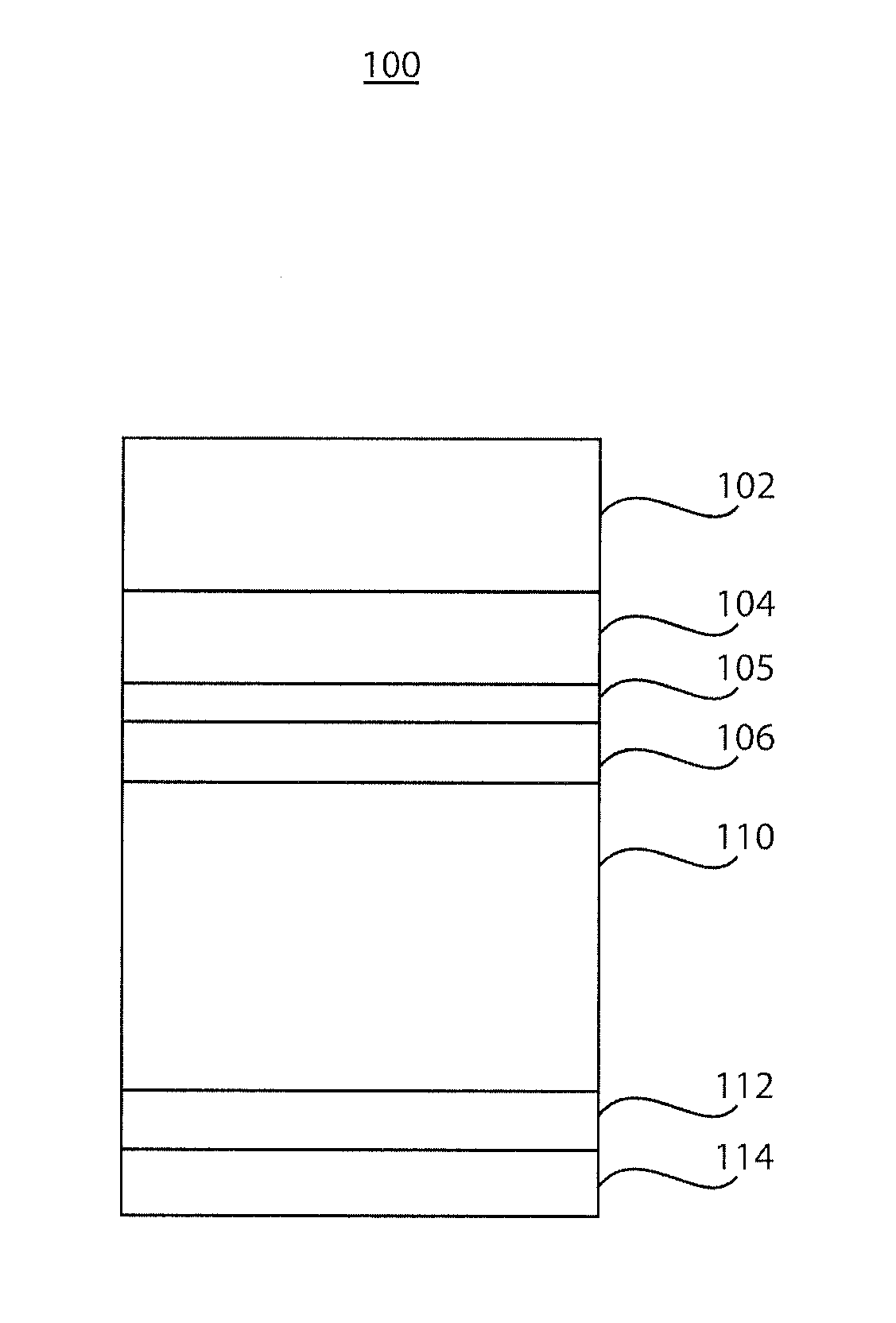
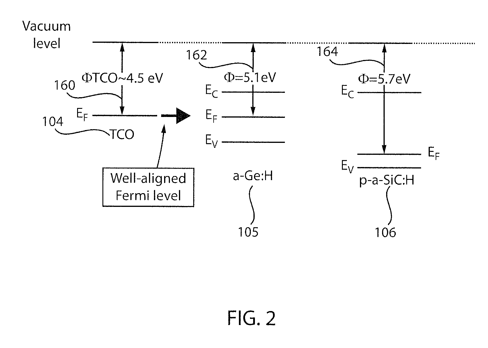
[0017]In accordance with the present principles, methods and devices are presented that provide light induced degradation resistance. Light induced degradation occurs in a semiconductor structure when the structure becomes saturated by incoming radiation (light soaked). The structure begins to degrade due in part to the reconfiguration of hydrogen atoms, which results in passivation and bond breaking between constituent materials. This degradation process becomes prominent if there exists a band offset at a p-i interface and / or at a transparent conductive oxide (TCO) to p+ interface.

[0018]A band offset describes the relative alignment (e.g., misalignment) of the energy bands between materials at a semiconductor heterojunction. Band offset at the TCO / p+ layer is unavoidable since all developed TCO films are n-type. In particularly useful embodiments, photovoltaic devices are constructed using materials and processes that reduce the risk of light-induced degradation. In one example, a...


PUM


Abstract

Methods for forming a photovoltaic device include forming a buffer layer between a transparent electrode and a p-type layer. The buffer layer includes a work function that falls substantially in a middle of a barrier formed between the transparent electrode and the p-type layer to provide a greater resistance to light induced degradation. An intrinsic layer and an n-type layer are formed over the p-type layer.

Description

RELATED APPLICATION INFORMATION[0001]This application is related to commonly assigned application Ser. No. ______, entitled: ENHANCING EFFICIENCY IN SOLAR CELLS BY ADJUSTING DEPOSITION POWER (Attorney Docket Number YOR920110767US1 (163-472)) filed concurrently herewith and incorporated herein by reference.BACKGROUND[0002]1. Technical Field[0003]The present invention relates to photovoltaic devices and methods for fabrication, and more particularly to devices, structures and fabrication methods that reduce light-induced degradation by setting a work function of a buffer layer.[0004]2. Description of the Related Art[0005]When a hydrogenated amorphous silicon solar cell (a-Si:H) is soaked in solar radiation, efficiency of the cell is degraded as soaking time increases. Such phenomenon has not been observed for other types of solar cells. This is called the Staebler-Wronski effect. According to conventional theory of the Staebler-Wronski effect (SW effect), hydrogen is reconfigured incr...

Claims


Application Information

Patent Timeline
IPC IPC(8): H01L31/0232H01L31/18
CPCH01L31/022466H01L31/075Y02E10/547Y02E10/548H01L31/1804Y02P70/50H01L31/03767
Inventor FOGEL, KEITH E.HONG, AUGUSTIN J.KIM, JEEHWANSADANA, DEVENDRA K.
Owner IBM CORP
Why Eureka
Try Eureka