Laminated ceramic electronic component

Inactive Publication Date: 2013-08-29
MURATA MFG CO LTD
View PDF8 Cites 22 Cited by
  • Summary
  • Abstract
  • Description
  • Claims
  • Application Information

AI Technical Summary

Problems solved by technology

The technique disclosed in Patent Document 1 may fail to deal with some of such cases, and as a result of thermal shock, laminated ceramic capacitors may suffer structural defects such

Method used


Image

  • Laminated ceramic electronic component
  • Laminated ceramic electronic component
  • Laminated ceramic electronic component

Examples


experimental example 1

[0040](1) Preparation of Samples

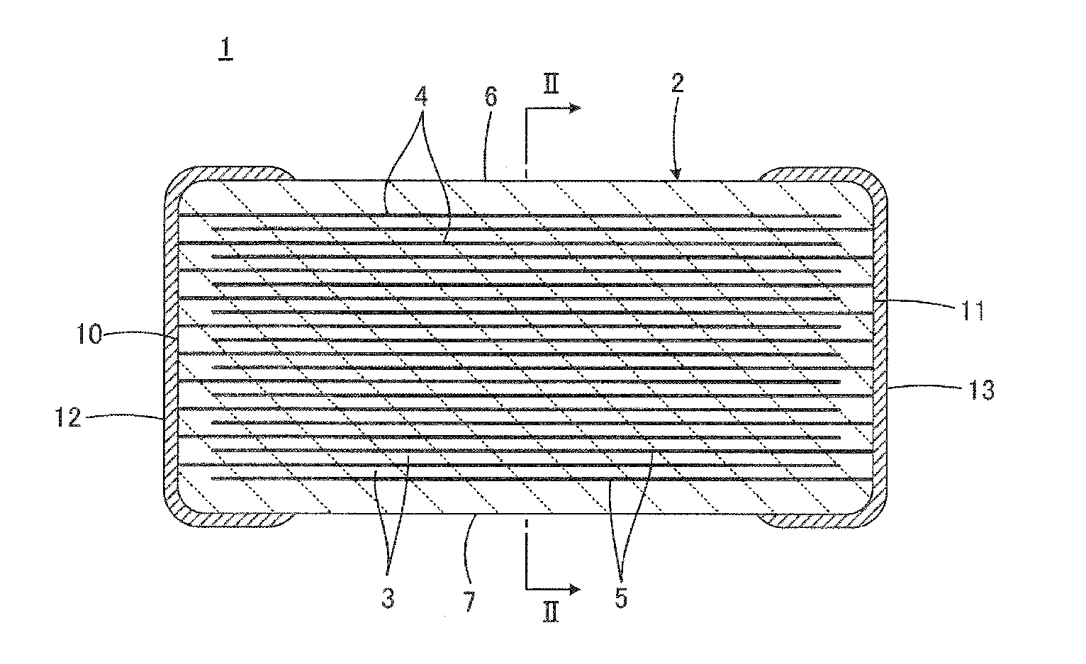
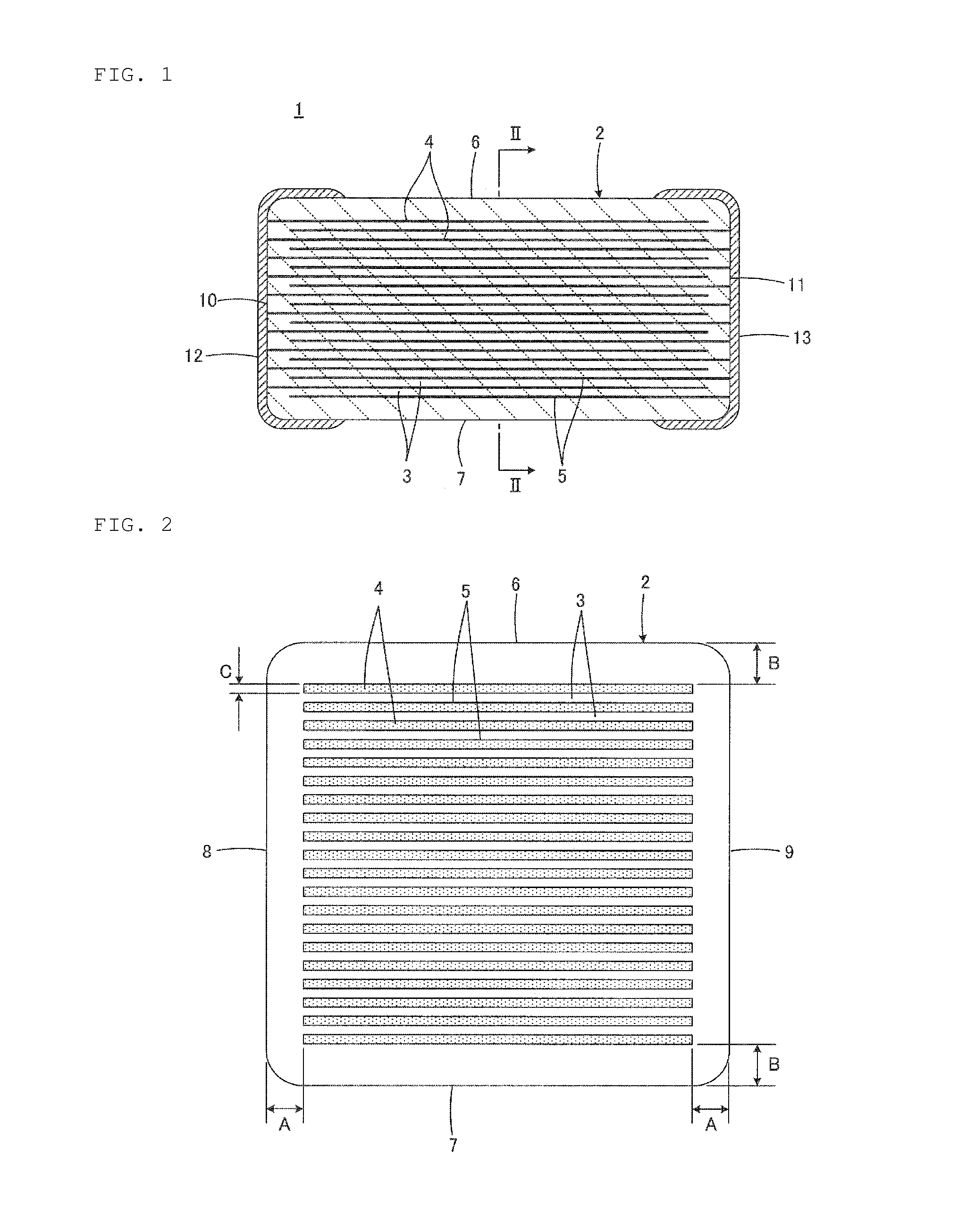
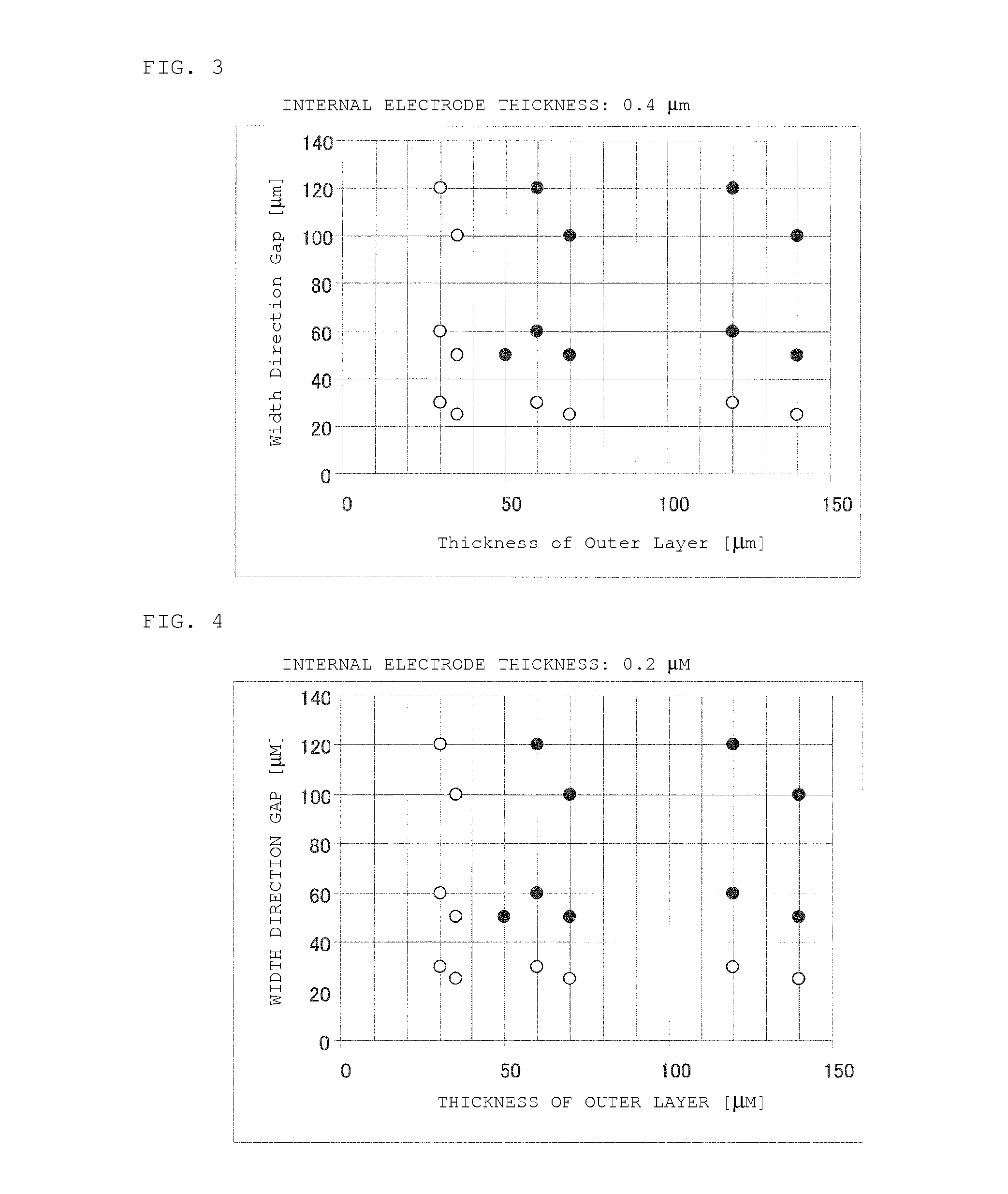
[0041]Ceramic green sheets including: ceramic powder containing barium titanate as its main constituent; and an organic binder were formed on base films so as to be 1 μm in thickness after firing. Then, conductive paste films to serve as internal electrodes were formed by screen printing onto the ceramic green sheets, so as to achieve the thickness shown in the column “Thickness of Internal Electrode” in Tables 1 and 2 after the firing. In this case, the dimensions of the printing pattern for the conductive paste films were adjusted so that internal electrodes were distributed in a region located with a width-direction gap interposed as shown in the column “Width-Direction Gap” in Tables 1 and 2, in laminated bodies obtained through subsequent cutting step and firing step.

[0042]Next, the green sheets with the conductive paste films formed thereon were stacked a predetermined number of times so as to alternate the sides to which the conductive paste fi...

experimental example 2

[0068]In Experimental Example 2, the relationship was evaluated between the coverage for internal electrodes and the defect generation ratio in a thermal shock test.

[0069]Through essentially the same steps as in the case of Experimental Example 1, laminated ceramic capacitors according to each sample were obtained which had the external dimensions shown in “Length Direction Dimension”, “Width Direction Dimension” and “Thickness Direction Dimension” of Table 3. The laminated ceramic capacitors according to each sample were all adjusted to 0.4 μm in the thickness of the internal electrode, 30 μm in width direction gap, and 35 μm in outer layer thickness. Then, the coverage for the internal electrodes was varied as shown in the column “Coverage” of Table 3, by controlling the maximum temperature in the firing step between 1100° C. and 1300° C.

[0070]For each of the obtained samples, the “Thickness of Internal Electrode”, “Width Direction Gap”, and “Outer Layer Thickness” were measured i...


PUM

PropertyMeasurementUnit
Fractionaaaaaaaaaa
Thicknessaaaaaaaaaa
Thicknessaaaaaaaaaa

Abstract

A laminated ceramic capacitor with a laminated body including a plurality of stacked ceramic layers and internal electrodes located between the ceramic layers. The laminated body has a pair of mutually opposed principal surfaces extending in the direction in which the ceramic layers extend, a pair of mutually opposed side surfaces and a pair of mutually opposed end surfaces which respectively extend in directions orthogonal to the principal surfaces. The internal electrodes are 0.4 μm or less in thickness, and are located in an area defined by a width-direction gap of 30 μm or less interposed with respect to each of the pair of side surfaces and an outer layer thickness of 35 μm or less interposed with respect to each of the pair of principal surfaces.

Description

CROSS REFERENCE TO RELATED APPLICATIONS[0001]The present application is a continuation of International application No. PCT / JP2011 / 077887, filed Dec. 2, 2011, which claims priority to Japanese Patent Application No. 2010-271097, filed Dec. 6, 2010, the entire contents of each of which are incorporated herein by reference.FIELD OF THE INVENTION[0002]This invention relates to a laminated ceramic electronic component, and more particularly, relates to an improvement for enhancing the thermal shock resistance of a laminated ceramic electronic component.BACKGROUND OF THE INVENTION[0003]For example, JP 2005-136132 A (Patent Document 1) discloses a technique for promoting the resistance of a laminated ceramic capacitor to thermal stress.[0004]More specifically, Patent Document 1 discloses a laminated ceramic capacitor including, as a main body section, a laminated body formed by arranging dielectric layers each between a plurality of internal electrodes to be stacked in the stacking direct...

Claims


Application Information

Patent Timeline
IPC IPC(8): H01G4/30
CPCH01G4/1209H01G4/012H01G4/30H01G4/005H01G4/12H01G4/258H05K1/162H05K3/1216H05K3/1291H05K3/4629H05K3/4664
Inventor SAITO, YOSHITOHIRATA, YOSUKEHIRAMATSU, TAKASHI
Owner MURATA MFG CO LTD
Why Eureka
Try Eureka