Method of Forming a Laminated Magnetic Core with Sputter Deposited and Electroplated Layers

a technology of laminated magnetic core and electroplating layer, which is applied in the direction of magnetic cores, transformers/inductances, magnetic bodies, etc., can solve the problems of increasing the stress of the stack, and sputter-deposited laminated magnetic cores

Active Publication Date: 2013-08-29
TEXAS INSTR INC
View PDF19 Cites 26 Cited by
  • Summary
  • Abstract
  • Description
  • Claims
  • Application Information

AI Technical Summary

Problems solved by technology

However, one drawback of sputter-deposited laminated magnetic cores is that it takes a significant amount of time to form a laminated magnetic core (e.g., two and one-half hours or more to form a core 10 μm thick).
Another drawback is that each layer in a sputter-deposited laminated magnetic core increases the stress of the stack.
Thus, thick laminated magnetic cores (e.g., 10 μm thick or thicker) formed by sputter deposition have significant stress levels which, in turn, substantially increase the likelihood of device failure.
One drawback of this approach is that the approach utilizes a different plating mold to form each magnetic layer.
The plating molds, in turn, are typically implemented as patterned photoresist layers, which are relatively expensive to form in a semiconductor fabrication process.
Thus, although faster, this approach is quite expensive.

Method used


Image

  • Method of Forming a Laminated Magnetic Core with Sputter Deposited and Electroplated Layers
  • Method of Forming a Laminated Magnetic Core with Sputter Deposited and Electroplated Layers
  • Method of Forming a Laminated Magnetic Core with Sputter Deposited and Electroplated Layers

Examples


Embodiment Construction

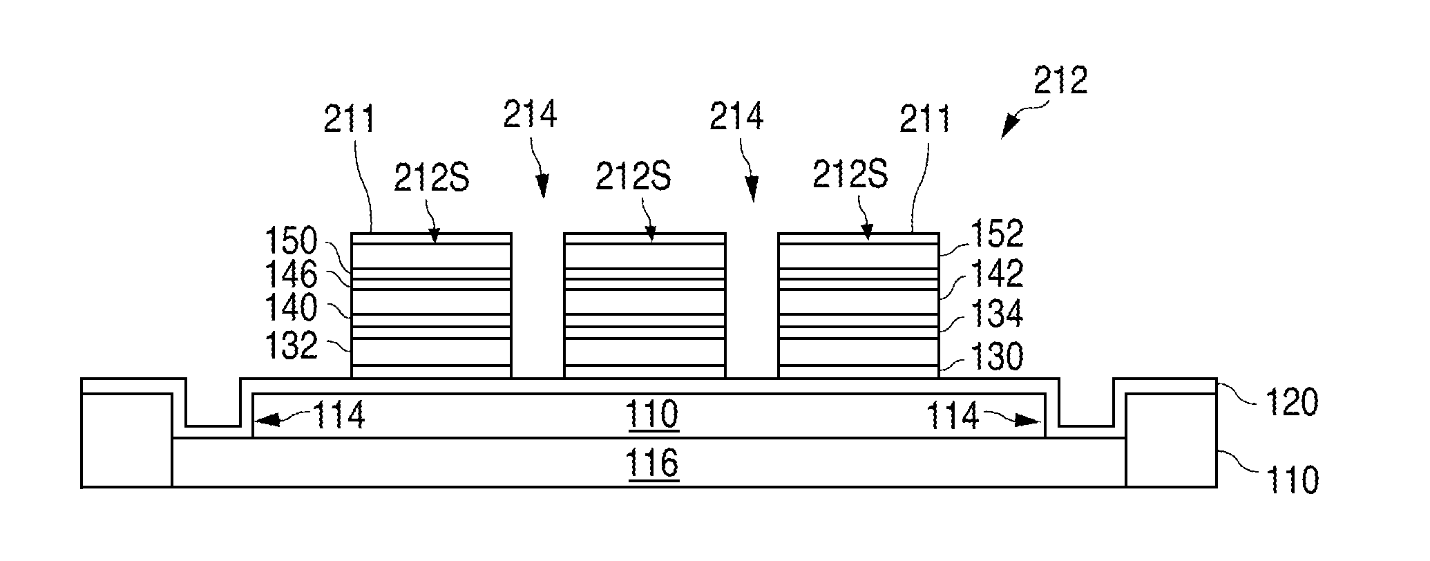
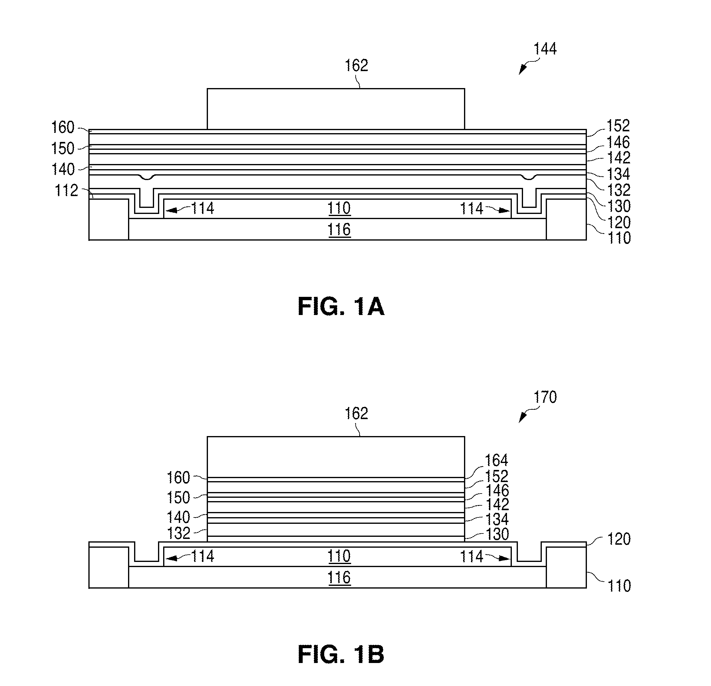
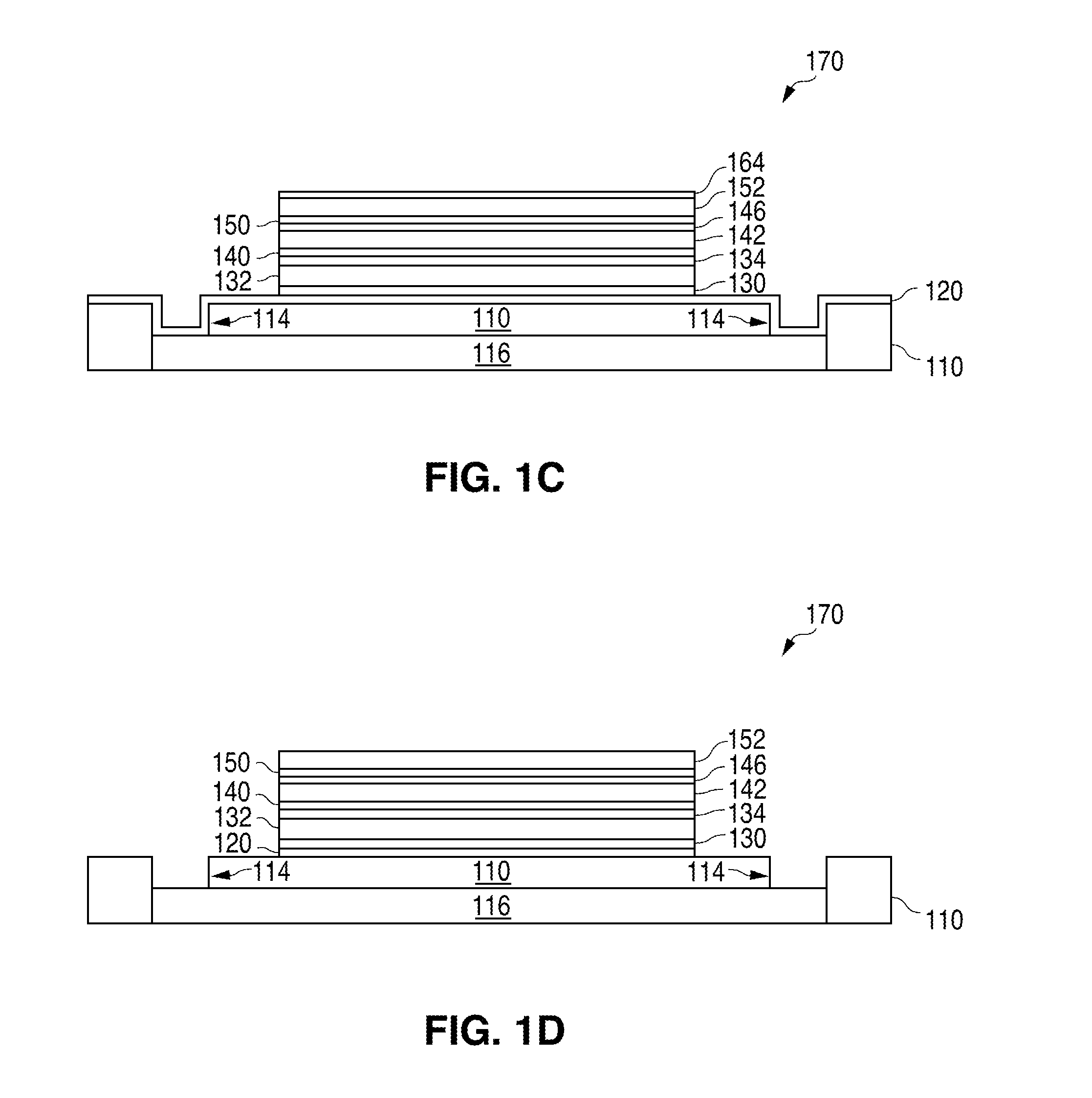
[0021]FIGS. 1A-1D show views that illustrate an example of a method of forming a laminated magnetic core in accordance with the present invention. Although the laminated magnetic core of the present invention is utilized in conjunction with a coil, the specifics of the coil are omitted for simplicity.

[0022]As shown in FIG. 1A, the method of the present invention utilizes a non-conductive structure 110 that has a substantially-planar top surface 112. Non-conductive structure 110 can be implemented with any material which has good dielectric properties. For example, a layer of photoimageable epoxy or polymer, such as SU-8, which has a relatively low stress and a low coefficient of thermal expansion, can be used. Materials such as SU-8 are substantially self planarizing.

[0023]In some embodiments, as illustrated in the present example, non-conductive structure 110 has openings 114 that expose underlying conductive structures 116, such as coil segments. (Only one conductive structure 116...


PUM

PropertyMeasurementUnit
deposition rateaaaaaaaaaa
thickaaaaaaaaaa
frequencyaaaaaaaaaa

Abstract

A laminated magnetic core, which has a number of magnetic layers and a number of insulation layers which are arranged so that an insulation layer lies between each vertically adjacent pair of magnetic layers, is formed in a method that forms the magnetic layers with an electroplating process, and the insulation layers with a sputter depositing process.

Description

BACKGROUND OF THE INVENTION[0001]1. Field of the Invention[0002]The present invention relates to laminated magnetic cores and, more particularly, to a method of forming a laminated magnetic core with sputter deposited and electroplated layers.[0003]2. Description of the Related Art[0004]An alternating current input to a coil generates an alternating magnetic field. One way to increase the strength of the magnetic field is to wrap the coil around a magnetic core, which is a structure that is formed from a material with a high magnetic permeability relative to air. In semiconductor fabrication processes, magnetic cores are commonly formed as thin-film structures by electroplating or sputter depositing a magnetic material.[0005]In a typical magnetic core electroplating process, a seed layer is first sputter deposited on a substantially-planar, non-conductive surface, followed by the formation of a plating mold (e.g., a patterned photoresist layer) on the seed layer. After this, a magne...

Claims


Application Information

Patent Timeline
Patent Type & Authority Applications(United States)
IPC IPC(8): H01L43/12C25D7/12
CPCC23C14/0617C23C14/185C25D7/123H01F10/265H01F27/24H01F41/046H01F41/26C25D7/001H01F3/00C23C28/00C23C28/321C23C28/34C23C28/42C23C28/44
Inventor LEE, DOK WONPAPOU, ANDREIFRENCH, WILLIAMHOPPER, PETER J.
Owner TEXAS INSTR INC
Why Eureka
Try Eureka