

Field stop structure, reverse conducting IGBT semiconductor device and methods for manufacturing the same
- Summary
- Abstract
- Description
- Claims
- Application Information
AI Technical Summary
Benefits of technology
Problems solved by technology
Method used
Image

Examples
first embodiment
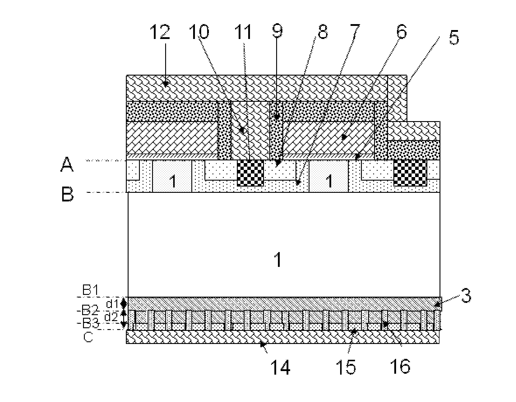
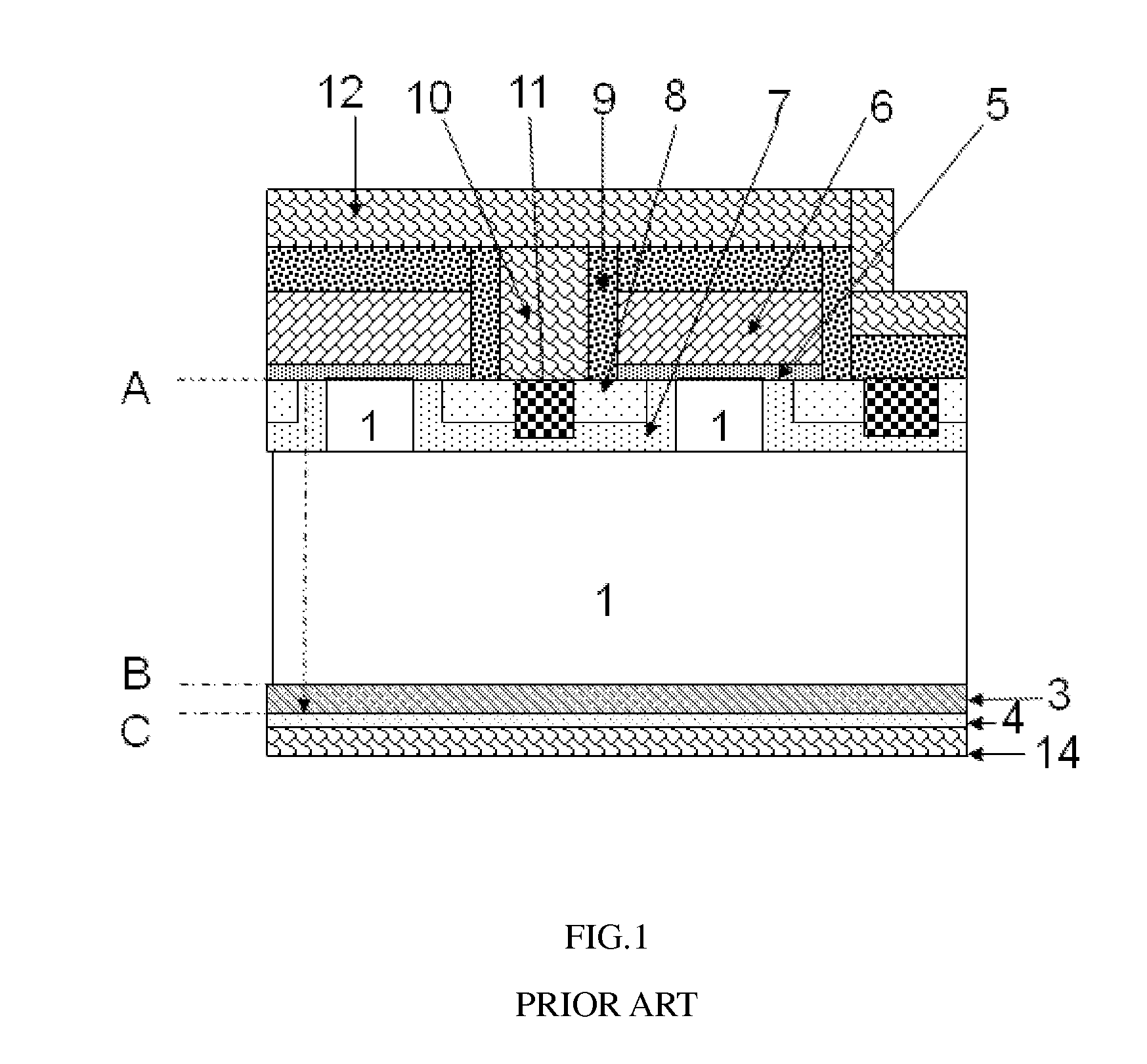
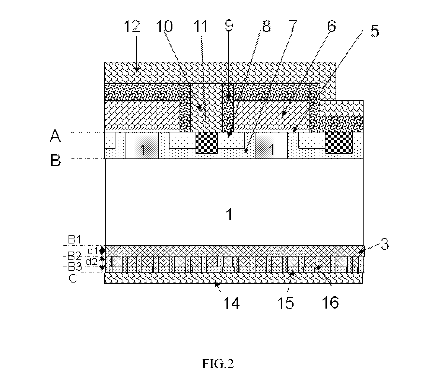
[0038]FIG. 2 illustrates a reverse conducting insulated gate bipolar transistor (IGBT) semiconductor device according to the present invention, which is integrated with an IGBT device and a fast recovered diode (FRD). In this embodiment, the IGBT device is a field-stop type IGBT (FSIGBT) with a reverse breakdown voltage of 1200 volts and an N-type drift region. Herein, in a FSIGBT with an N-type drift region, N-type is defined as a first conductivity type and P-type is defined as a second conductivity type. In other embodiments, the IGBT device may be a FSIGBT with a P-type drift region, and similarly, in which P-type is defined as the first conductivity type and N-type is defined as the second conductivity type. As P-type FSIGBTs have similar features with N-type FSIGBTs, those embodiments in relation to P-type FSIGBTs will not be further specified herein.
[0039]In the first embodiment, the reverse conducting IGBT semiconductor device includes trenches formed on a back side of an N-...
second embodiment
[0062]In the present invention, more integrations can be realized between front-side and back-side processes adopted in the method for manufacturing a reverse conducting IGBT semiconductor device. Steps of the method will be specified in details in the following description.
[0063]In a first step, as illustrated in FIG. 3A, an N-type silicon substrate 1 with a dopant concentration C1 of 2.4e13 cm−3, a resistivity of 90 Ω·cm and a thickness of greater than 700 μm is provided.
[0064]Thereafter, front-side processes similar with those known by those skilled in the art of VDMOS are carried out, including: forming gate oxide 5 and a polysilicon gate 6 on top of the silicon substrate 1; and forming a P-well 7 and an N+ source 8. Alternatively, before the formation of the gate oxide 5 and other subsequent front-side processes, an N-type epitaxial layer may be first formed over a front side surface of the silicon substrate 1.
[0065]Next, a first dielectric film (not shown) is deposited over th...
third embodiment
[0079]In the present invention, a method for manufacturing a reverse conducting IGBT semiconductor device can be implemented with a reduced process complexity. Steps of the method will be specified in details in the following description with reference to FIG. 2.
[0080]In a first step, an N-type silicon substrate 1 with a dopant concentration C1 of 2.4e13 cm−3, a resistivity of 90 Ω·cm and a thickness of greater than 700 μm is first provided. After that, a first dielectric film (not shown) is deposited over a front side of the silicon substrate 1 so as to protect the front side. In this embodiment, the first dielectric film is an oxide film and has a thickness of 5000 Å to 20000 Å.
[0081]Next, the back side of the N-type silicon substrate 1 is grinded to a desired thickness of 500 μm to 700 μm. Herein, in FIG. 2, the cross section A represents a plane of the front side of the silicon substrate 1 whilst the cross section C represents a plane of the back side surface of the grinded sili...
PUM
 Abstract
Description
Claims
Application Information