Semiconductor package, semiconductor apparatus and method for manufacturing semiconductor package
Active Publication Date: 2013-09-26
SHINKO ELECTRIC IND CO LTD
View PDF4 Cites 52 Cited by
Summary
Abstract
Description
Claims
Application Information
AI Technical Summary
This helps you quickly interpret patents by identifying the three key elements:
Problems solved by technology
Method used
Benefits of technology
Benefits of technology
The present invention provides a semiconductor package and a method of manufacturing the package to address the problem of warpage, where a semiconductor chip and a metal plate become warped during the bonding process. The semiconductor chip and metal plate are surrounded by insulating layers to prevent any warping. The thickness of the metal plate is thinner than that of the semiconductor chip, and the side surface of the metal plate is covered by the insulating layers. The method includes steps of forming insulating layers on a support substrate, bonding the semiconductor chip onto the metal plate, and then removing the support substrate. This invention reduces warrike and improves the manufacturing of semiconductor packages.
Problems solved by technology
Thus, warpage occurs in the semiconductor package due to the stress release.
Method used
Image
Click on the blue label to locate the original text in one second.
Reading with bidirectional positioning of images and text.
Examples
first embodiment
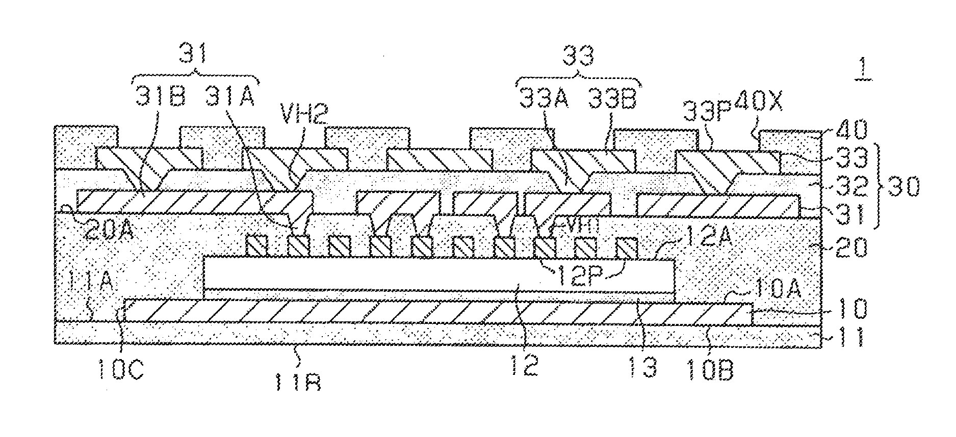
[0036]Hereinafter, a first embodiment will be described referring to FIGS. 1A and 1B to FIGS. 4A to 4D.
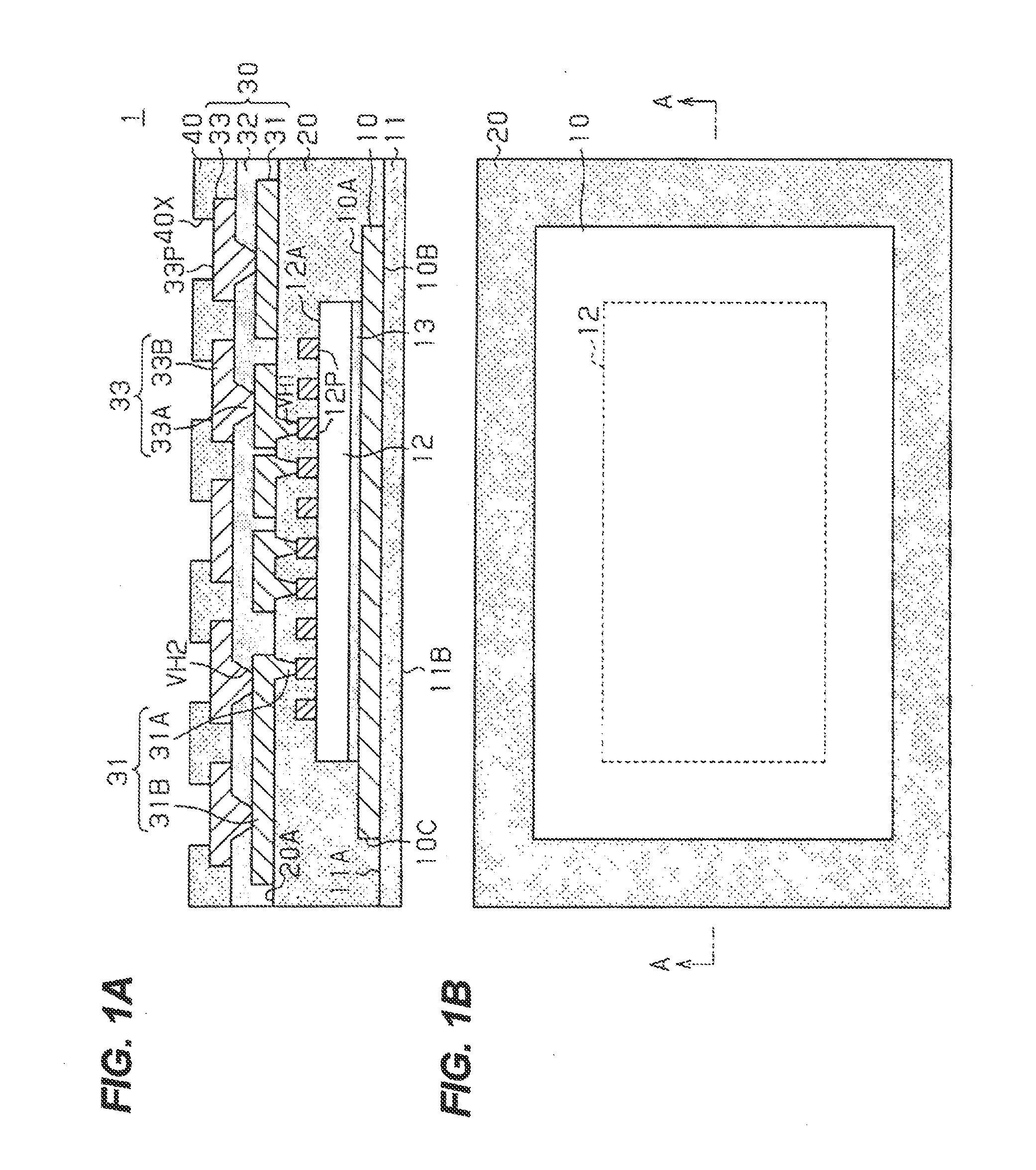
[0037]As shown in FIG. 1A, a semiconductor package 1 includes a metal plate 10, a first insulating layer 11, a semiconductor chip 12, a second insulating layer 20, a wiring structure 30, and a solder resist layer 40.
[0038]The metal plate 10 includes a first surface 10A (upper surface in FIG. 1A), a second surface 10B (lower surface in FIG. 1A) opposite to the first surface 10A, and a side surface 10C between the first surface 10A and the second surface 10B. The thickness of the metal plate 10 is set to be thinner than that of the semiconductor chip 12. Specifically, it is preferable that the thickness of the metal plate 10 be about 50 to 95% of the thickness of the semiconductor chip 12, for example, from the viewpoint of warpage reduction of the semiconductor package 1. More specifically, the thickness of the metal plate 10 may be set to about 15 to 70 μm, for example. As shown in...
second embodiment
[0087]Hereinafter, a second embodiment will be now described with reference to FIGS. 5A and 5B to FIG. 9. A semiconductor package 1A according to this embodiment is different from the first embodiment in that a connection pad 50P connected to a first wiring layer 31 is formed on the same plane as a metal plate 10. Hereinafter, different points from the first embodiment will be mainly described. The same reference numerals are given to the same members as the members shown in FIGS. 1A and 1B to FIGS. 4A to 4D, and detailed description thereof will be omitted.
[0088]As shown in FIG. 5A, on a first surface 11A of a first insulating layer 11, a metal plate 10 is formed, and a conductive layer 50 that is electrically separated from the metal plate 10 is also formed. As shown in FIG. 5B, the metal plate 10 is formed over approximately the entire surface excluding an outer edge of the semiconductor package 1A (for example, the first insulating layer 11 shown in FIG. 5A), and is formed to ex...
third embodiment
[0116]Hereinafter, a third embodiment will be now described with reference to FIGS. 10 to 13. A semiconductor package 1B of the present embodiment is different from the first embodiment in that a connection pad 51P connected to a first wiring layer 31 is provided in an intermediate position in a thickness direction of a second insulating layer 20. Hereinafter, different points from the first embodiment will be mainly described. The same reference numerals are given to the same members as the members shown in FIGS. 1A and 1B to FIG. 9, and detailed description thereof will be omitted.
[0117]The second insulating layer 20 includes an insulating layer 23 and an insulating layer 24. As materials of the insulating layers 23 and 24, for example, a thermosetting epoxy-based insulating resin may be used. The insulating resin is not limited to the thermosetting resin, and a photosensitive insulating resin may be used.
[0118]The insulating layer 23 is formed to cover a first surface 11A of an i...
PUM
Abstract
A semiconductorpackage includes: a metal plate including a first surface, a second surface and a side surface; a semiconductorchip on the first surface of the metal plate, the semiconductorchip comprising a first surface, a second surface and a side surface; a first insulating layer that covers the second surface of the metal plate; a second insulating layer that covers the first surface of the metal plate, and the first surface and the side surface of the semiconductor chip; and a wiring structure on the second insulating layer and including: a wiring layer electrically connected to the semiconductor chip; and an interlayer insulating layer on the wiring layer. A thickness of the metal plate is thinner than that of the semiconductor chip, and the side surface of the metal plate is covered by the first insulating layer or the second insulating layer.
Description
[0001]This application claims priority from Japanese Patent Application No. 2012-063947, filed on Mar. 21, 2012, the entire contents of which are herein incorporated by reference.BACKGROUND[0002]1. Technical Field[0003]The present disclosure relates to a semiconductor package, a semiconductor apparatus and a method for manufacturing the semiconductor package.[0004]2. Description of the Related Art[0005]In the related art, a semiconductor package including a semiconductor chip and a resin layer that covers the semiconductor chip has been used.[0006]As an example of such a semiconductor package, a structure has been proposed in which an active surface (circuit forming surface) and a side surface of a semiconductor chip are covered by an insulating layer and a wiring structure electrically connected to the semiconductor chip is formed on the insulating layer (for example, see JP-A-2011-119502 and JP-A-2008-300854).[0007]As a method for manufacturing such a semiconductor package, the fo...
Claims
Application Information
Patent Timeline
Application Date:The date an application was filed.
Publication Date:The date a patent or application was officially published.
First Publication Date:The earliest publication date of a patent with the same application number.
Issue Date:Publication date of the patent grant document.
PCT Entry Date:The Entry date of PCT National Phase.
Estimated Expiry Date:The statutory expiry date of a patent right according to the Patent Law, and it is the longest term of protection that the patent right can achieve without the termination of the patent right due to other reasons(Term extension factor has been taken into account ).
Invalid Date:Actual expiry date is based on effective date or publication date of legal transaction data of invalid patent.

