Capacitor and method for manufacturing the same

a technology of capacitors and manufacturing methods, applied in the manufacture of capacitors, variable capacitors, fixed capacitors, etc., can solve the problems of low connection resistance, low connection reliability, and low connection resistance, so as to reduce the internal resistance of elements, reduce the reliability of connection, and reduce the effect of connection resistan

Active Publication Date: 2013-09-26
NIPPON CHIMI CON CORP
View PDF2 Cites 15 Cited by
  • Summary
  • Abstract
  • Description
  • Claims
  • Application Information

AI Technical Summary

Benefits of technology

[0008]In the structure providing current collector plates for each end-face of wound elements, it is necessary to ensure connection, distance between external terminals of the anode and cathode sides and current collector plates if the external terminals are placed, so as to be adjacent to outer packaging members that cover the outsides of wound elements. Also, inner and outer sides of wound elements have different distribution of the internal resistance. Thus, courses for this are needed, and it is necessary to pay attention to connection between elements and current collector plates. The structure using current collector plates can reduce internal resistance of elements. However, the reliability of the connection may be reduced and / or the connection resistance may get high according to stress that is applied in the middle of the manufacture to current collector plates intervening between external terminals and elements.
[0009]As to such connection, there is a little space between capacitor elements and sealing members. If this space is enlarged so that clearance necessary for connection members and the connection is increased, the resistance is increased as much as the clearance is increased, and the size of the height of capacitors also increases. If this clearance (distance) is decreased, the space is narrowed so that capacitors can become compact. However, this brings problems of troublesome connection and incomplete connection because clearance for the connection between capacitor elements and sealing members is decreased.
[0013]It is therefore an object of the present invention to achieve reduction of the resistance, the simple and robust connection structure, and facile connection of capacitors in view of the above problems.
[0014]It is another object of the present invention to provide capacitors of good accuracy of welding and of increased connection strength between current collector plates and external terminal members without being affected by the accuracy of processing of the current collector plates and the external terminal members in view of the above problems.

Problems solved by technology

However, the reliability of the connection may be reduced and / or the connection resistance may get high according to stress that is applied in the middle of the manufacture to current collector plates intervening between external terminals and elements.
However, this brings problems of troublesome connection and incomplete connection because clearance for the connection between capacitor elements and sealing members is decreased.
However, if the accuracy of processing current collector plates and external terminal members is low because the accuracy of the shape of each current collector plate and external terminal member is different from each other etc., gaps are generated between contact faces of current collector plates and external terminal members.
A problem in a case where such contact faces between which gaps are generated are irradiated with laser beams or electron beams is that gaps vary welded areas to make the accuracy of the welding worse.
A problem in a case where gaps between contact faces are large is that welded ranges are narrowed, connection strength between current collector plates and external terminal members is decreased, the connection resistance gets higher, etc.

Method used


Image

  • Capacitor and method for manufacturing the same
  • Capacitor and method for manufacturing the same
  • Capacitor and method for manufacturing the same

Examples


first embodiment

[0059]The first embodiment is the structure of connecting external terminals to current collector plates, which are connected to an element end-face of a capacitor element, and forming the external terminals on the capacitor element.

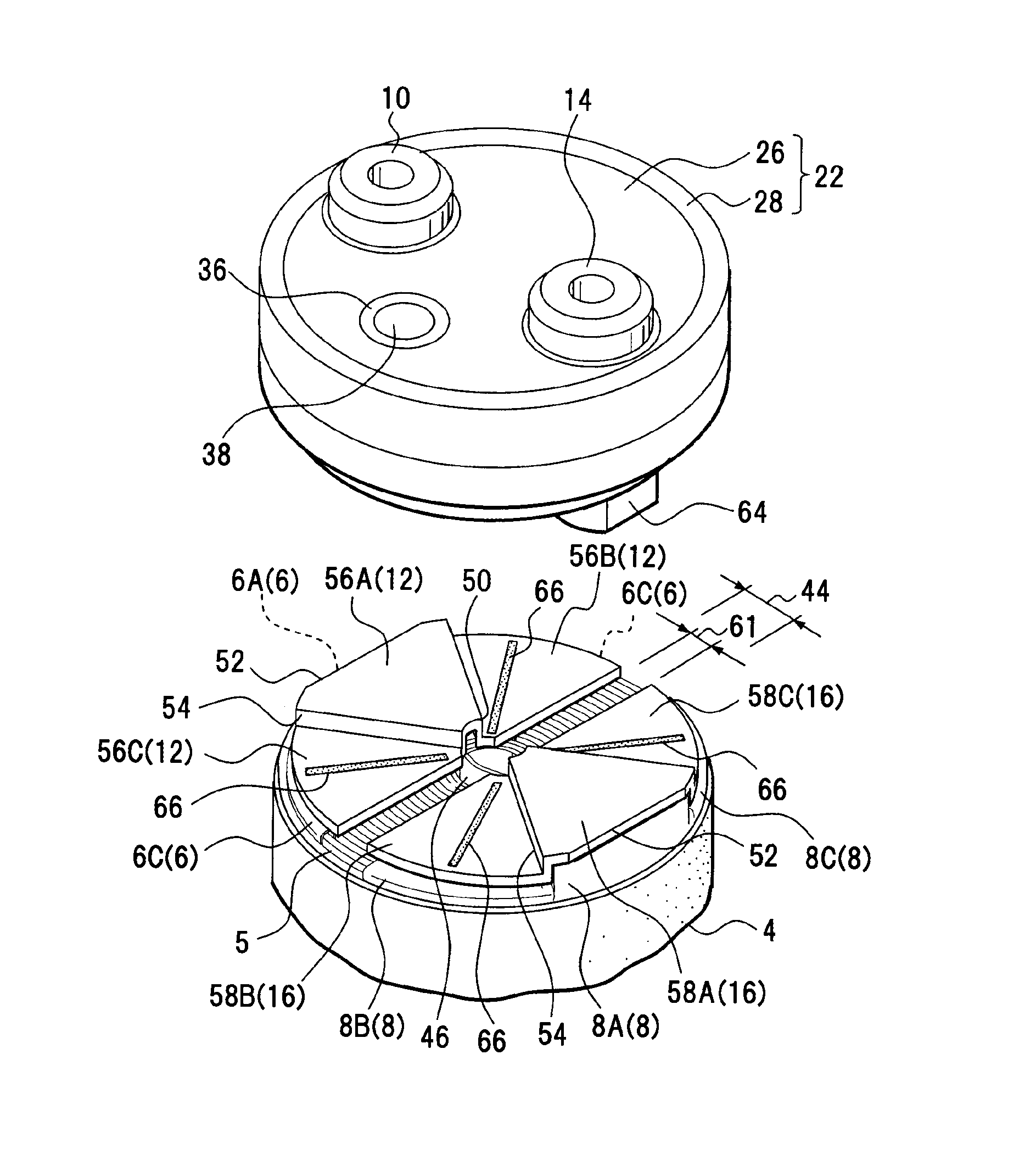
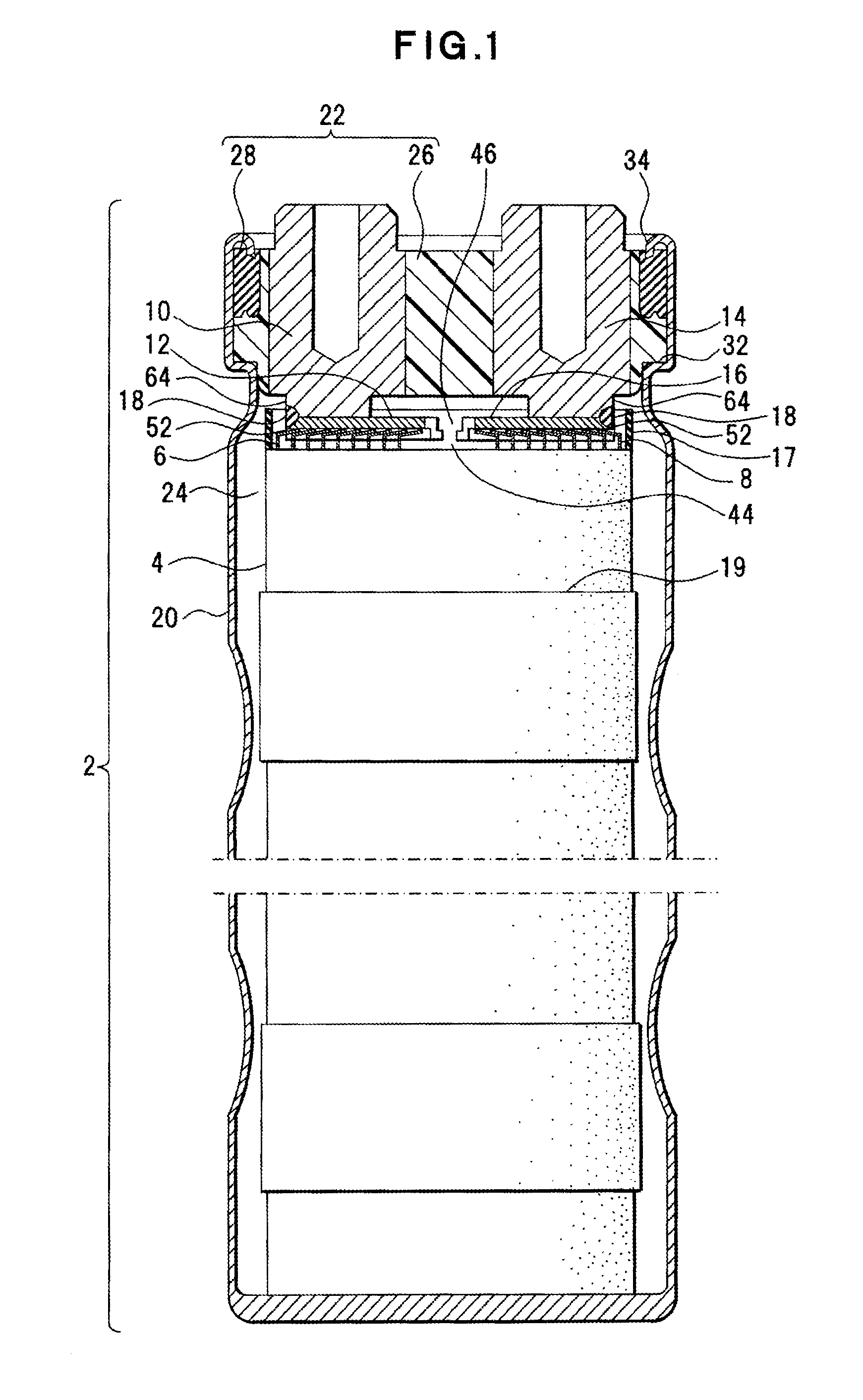
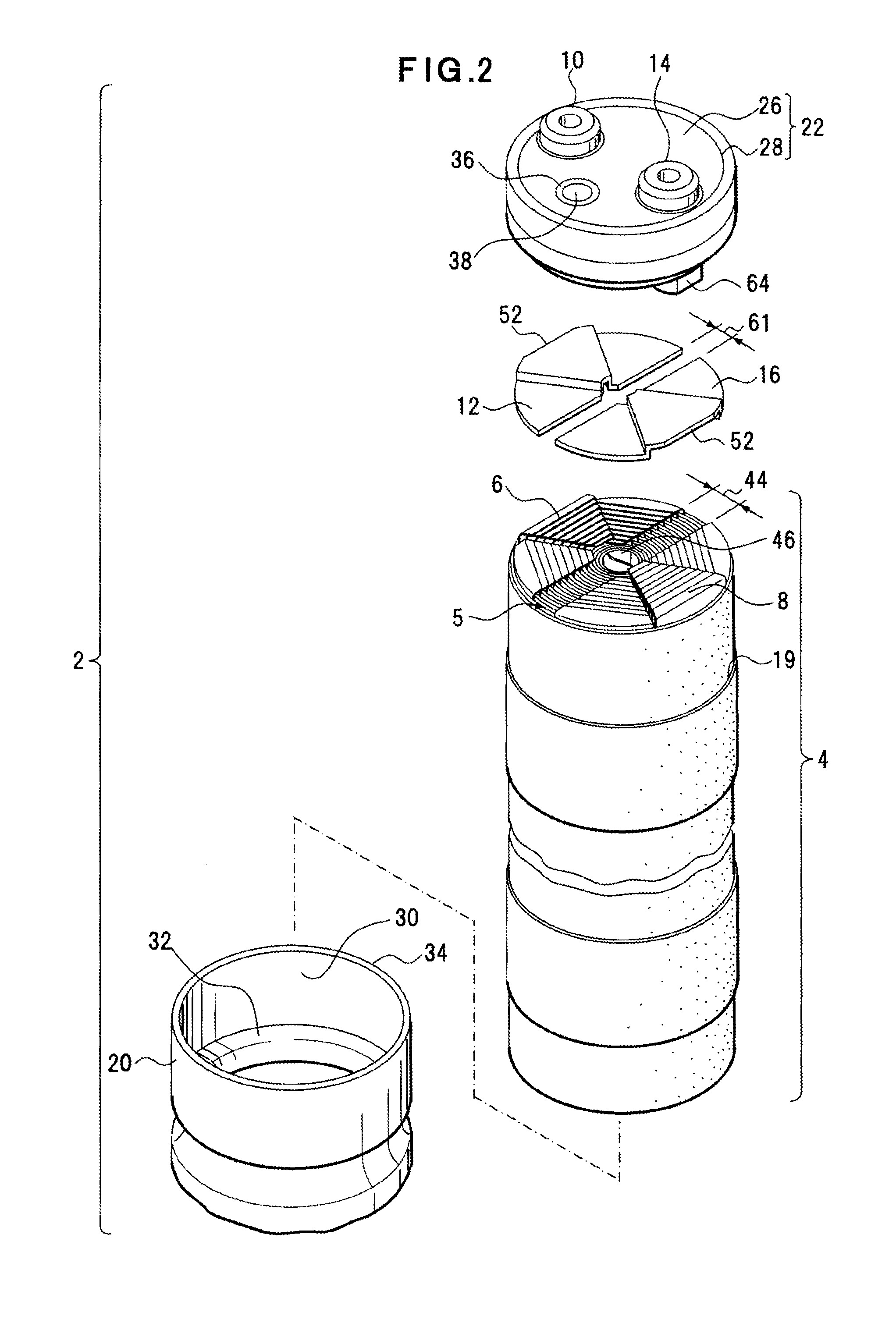
[0060]FIGS. 1 and 2 will be referred to concerning the first embodiment. FIG. 1 represents a longitudinal cross-section depicting an example of an electric double layer capacitor and FIG. 2 depicts an example of the electric double layer capacitor, which is partially exploded.

[0061]This electric double layer capacitor 2 is an example of the capacitor of the present invention. As depicted in FIG. 1, an anode part 6 and a cathode part 8 are formed over one element end-face of a capacitor element 4 in this electric double layer capacitor 2. Each anode part 6 and cathode part 8 is an example of an electrode protrusion, and is constituted by part of an electrode body (anode body 60 and cathode body 80: FIG. 3) that is drawn from an element end-face 5 of the c...

second embodiment

[0105]The second embodiment discloses a method for manufacturing the above described capacitor.

[0106]FIGS. 9A, 9B, 10A and 10B will be referred to concerning the second embodiment. FIG. 8 is a flowchart depicting an example of every manufacturing step of electric double layer capacitors according to the second embodiment. FIGS. 9A and 9B depict molded states of an anode part and a cathode part, and FIGS. 10A and 10B depict welding steps of current collector plates and a capacitor element by laser.

[0107]A series of these manufacturing steps is an example of the method for manufacturing a capacitor of the present invention, and as depicted in FIG. 8, includes a forming step of the capacitor element 4 and electrode parts (electrode protrusions) (step S11), a molding step of the anode part 6 and the cathode part 8 (step S12), a first connecting step (step S13), a second connecting step (step S14) and an impregnating with electrolyte and sealing step (step S15).

[0108](1) Forming Step of ...

third embodiment

[0121]In the third embodiment, arrangement of external terminals and forms of current collector plates are disclosed.

[0122]FIGS. 11A and 11B will be referred to concerning the third embodiment. FIGS. 11A and 11B depict the connection between current collector plates and external terminals according to the third embodiment. FIG. 11A depicts the state before the connection. FIG. 11B depicts laser irradiation during the connection.

[0123]The anode terminal 10 and the cathode terminal 14 that are disposed in the sealing plate 22 in this embodiment are arranged on the element end-face 5 of the capacitor element 4 in the vicinity of the winding center 46 as depicted in FIG. 11A. The terminal side connecting face 64 of each anode terminal 10 and cathode terminal 14 is back toward the winding center 46 further than the outer circumference of the capacitor element 4.

[0124]In this embodiment, as depicted in FIG. 11A, a recess 70 that is back toward the winding center 46 is formed in each termi...


PUM

PropertyMeasurementUnit
nugget depthaaaaaaaaaa
bending angleaaaaaaaaaa

Abstract

A capacitor includes a capacitor element that is a wound element or an element other than the wound element, and that includes electrode bodies each of which is in an anode side and a cathode side, and separators that intervenes between the electrode bodies; a sealing member that seals an opening of a case member accommodating the capacitor element; at least one electrode protrusion that protrudes from one of the electrode bodies on an element end-face of the capacitor element, at least one of current collector plate that is connected to the electric protrusion; and at least one terminal member that is disposed in the sealing member, and is superposed on the current collector plate, a side face part of the terminal member being welded to a side face part of the current collector plate.

Description

CROSS-REFERENCE TO RELATED APPLICATIONS[0001]This application is a continuation of International Application No. PCT / JP2011 / 006266, filed on Nov. 9, 2011, which is entitled to the benefit of priority of Japanese Patent Application No. 2010-251352, filed on Nov. 9, 2010, Japanese Patent Application No. 2010-251355, filed on Nov. 9, 2010, Japanese Patent Application No. 2010-251356, filed on Nov. 9, 2010, Japanese Patent Application No. 2011-035484, filed on Feb. 22, 2011, Japanese Patent Application No. 2011-160248, filed on Jul. 21, 2011, and Japanese Patent Application No. 2011-160247, filed on Jul. 21, 2011, the contents of which are hereby incorporated by reference.BACKGROUND OF THE INVENTION[0002]i) Field of the Invention[0003]The present invention relates to connection between capacitor elements and external terminals that are in sealing members sealing openings of outer packaging members of capacitor elements, and relates to capacitors that use laser welding for their connecti...

Claims


Application Information

Patent Timeline
Patent Type & Authority Applications(United States)
IPC IPC(8): H01G4/01H01G13/00H01G4/32
CPCH01G9/008H01G9/04H01G4/01Y10T29/435H01G13/00Y02E60/13H01G4/32
Inventor MORI, MASAYUKIKUBOUCHI, TATSUOFURUSAWA, AKIHIRO
Owner NIPPON CHIMI CON CORP
Why Eureka
Try Eureka