Supercharge Your Innovation With Domain-Expert AI Agents!

METHOD FOR PRODUCING Ga-CONTAINING GROUP III NITRIDE SEMICONDUCTOR

a nitride semiconductor and group iii technology, applied in semiconductor/solid-state device manufacturing, basic electric elements, electric devices, etc., can solve the problem of large reduce the density of occurrence origin of threading dislocation, and reduce the density of buffer layer crystal nucleus density , the effect of reducing the density of occurrence origin

Active Publication Date: 2013-10-03
TOYODA GOSEI CO LTD
View PDF2 Cites 3 Cited by
  • Summary
  • Abstract
  • Description
  • Claims
  • Application Information

AI Technical Summary

Benefits of technology

The present invention aims to reduce the threading dislocation density in semiconductor materials by reducing the density of threading dislocation origin. The invention proposes a method that involves heat-treating a substrate with a buffer layer formed thereon to reduce crystal nucleus density and conform the crystal nuclei to the lattice structure of the buffer layer, resulting in a reduction of threading dislocation density in the semiconductor material that is to be grown. The heat treatment is carried out at a temperature higher than the temperature at which the semiconductor material grows on the buffer layer, and the density of semiconductor crystal grains is increased during the heat treatment. This results in a decrease in the density of threading dislocation occurrence in the semiconductor material.

Problems solved by technology

As a result, density of occurrence origin of threading dislocation is still large.

Method used


Image

  • METHOD FOR PRODUCING Ga-CONTAINING GROUP III NITRIDE SEMICONDUCTOR
  • METHOD FOR PRODUCING Ga-CONTAINING GROUP III NITRIDE SEMICONDUCTOR
  • METHOD FOR PRODUCING Ga-CONTAINING GROUP III NITRIDE SEMICONDUCTOR

Examples


example 1

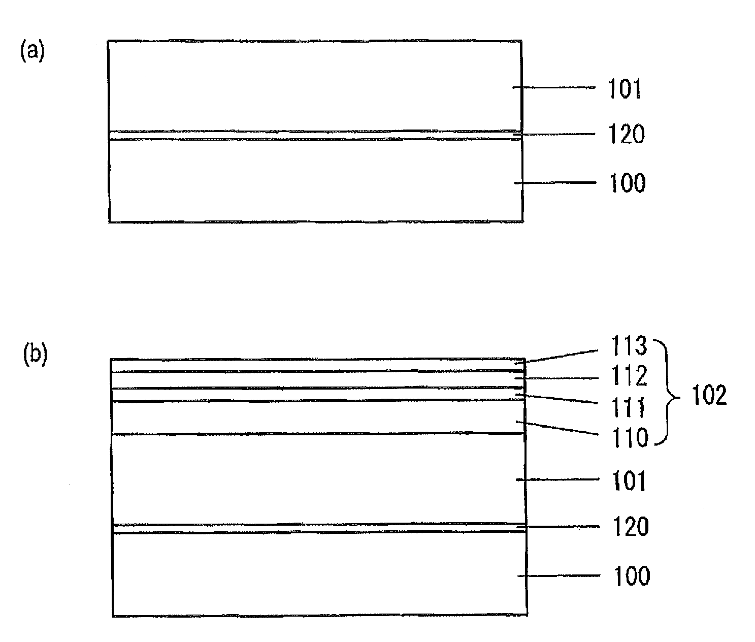
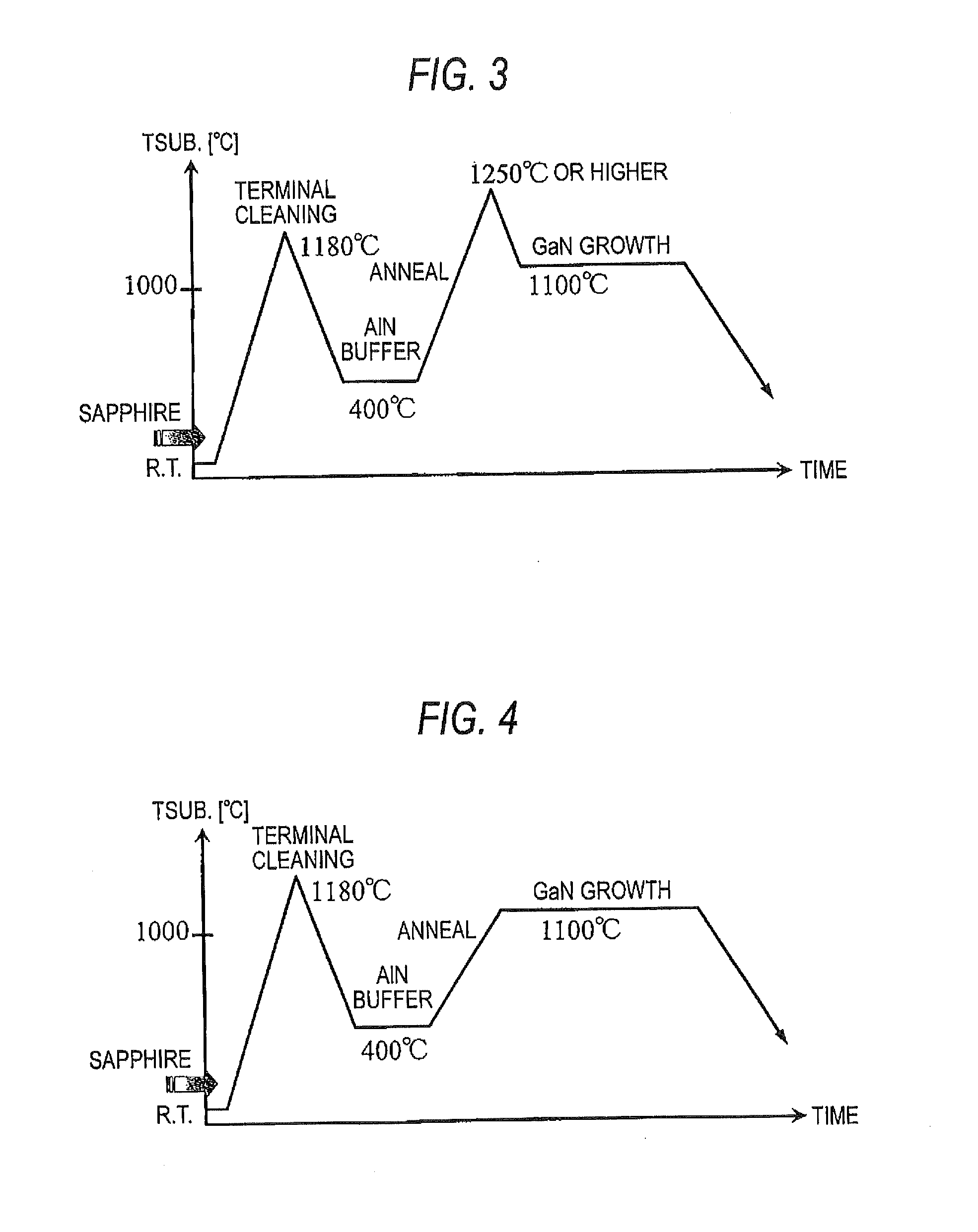
[0028]This example is an example that a buffer layer comprising AlN was formed on a sapphire substrate having c surface as a principal surface by an MOCVD method, and after heat treatment, GaN was grown. The crystal growth method is a metal organic chemical vapor deposition method (MOCVD method). A gas used is as follows. Hydrogen or nitrogen (H2 or N2) was used as a carrier gas, ammonia gas (NH3) was used as a nitrogen source, trimethyl gallium (Ga(CH3)3: hereinafter referred to as “TMG”) was used as a Ga source, and trimethyl aluminum (Al(CH3)3: hereinafter referred to as “TMA”) was used as an Al source.

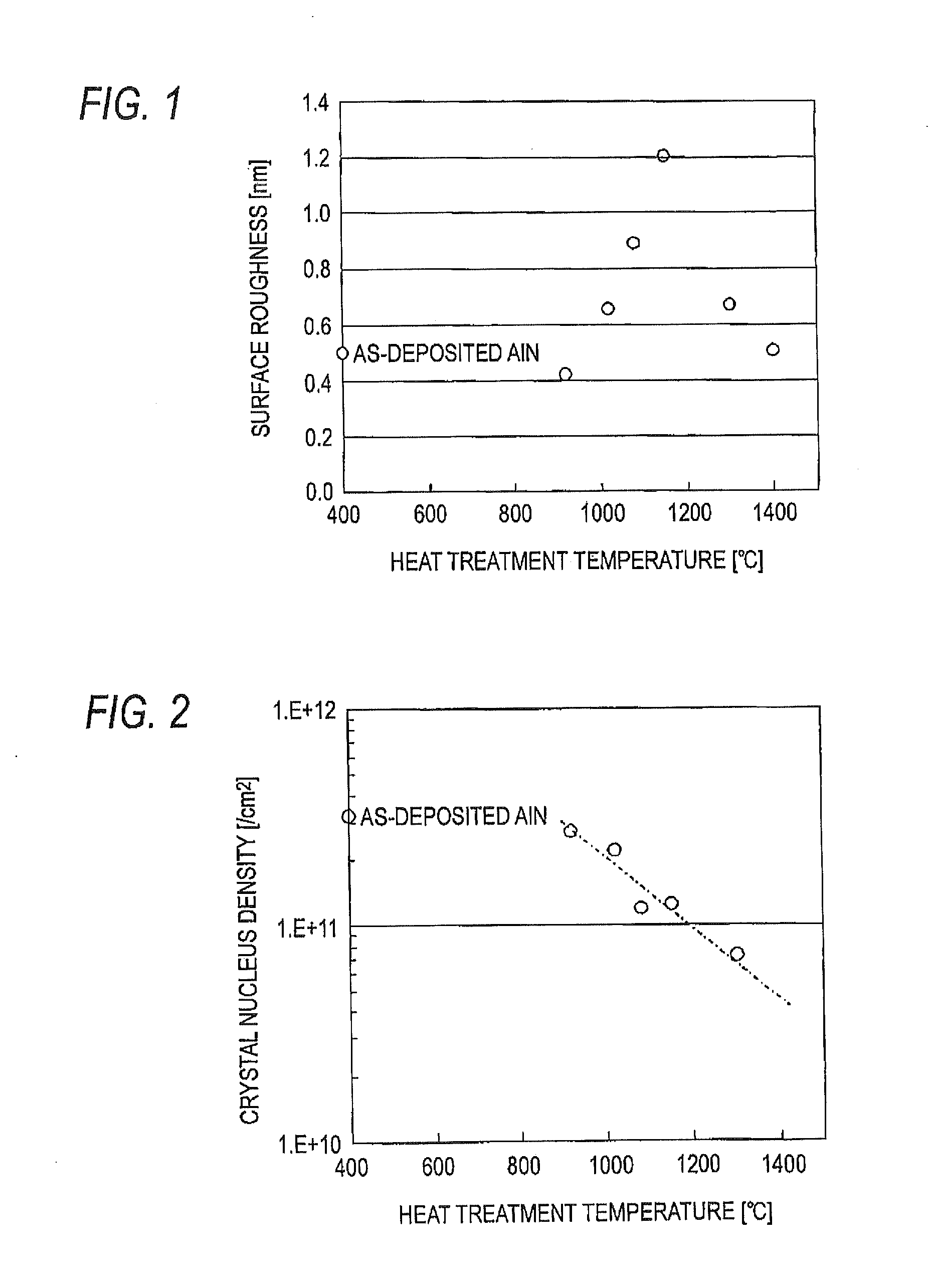
[0029]Change of crystal nucleus by heat treatment of a buffer layer is described. A sapphire substrate was placed in an MOCVD apparatus, a substrate temperature was increased to 1,180° C. from room temperature while flowing hydrogen gas, thereby heating and cleaning the sapphire substrate, and attached matters on the surface of the sapphire substrate were removed. The substrate tem...


PUM

PropertyMeasurementUnit
temperatureaaaaaaaaaa
thicknessaaaaaaaaaa

Abstract

A method for producing a Ga-containing group III nitride semiconductor having reduced threading dislocation is disclosed. A buffer layer in a polycrystal, amorphous or polycrystal / amorphous mixed state, comprising AlGaN is formed on a substrate. The substrate having the buffer layer formed thereon is heat-treated at a temperature higher than a temperature at which a single crystal of a Ga-containing group III nitride semiconductor grows on the buffer layer and at a temperature that the Ga-containing group III nitride semiconductor does not grow, to reduce crystal nucleus density of the buffer layer as compared with the density before the heat treatment. After the heat treatment, the temperature of the substrate is decreased to a temperature that the Ga-containing group III nitride semiconductor grows, the temperature is maintained, and the Ga-containing group III nitride semiconductor is grown on the buffer layer.

Description

BACKGROUND OF THE INVENTION[0001]1. Field of the Invention[0002]The present invention relates to a method for producing a Ga-containing group III nitride semiconductor having reduced threading dislocation.[0003]2. Description of the Related Art[0004]A method of forming a low temperature buffer layer on a sapphire substrate by a metal organic chemical vapor deposition method (hereinafter referred to as an “MOCVD method”) and growing GaN on the buffer layer has conventionally been known.[0005]For example, in JP-A-2005-19872, a sapphire substrate is heat-treated at 1,135° C. to clean the surface thereof, a substrate temperature is decreased to 515° C., a buffer layer comprising GaN having a thickness of 20 nm is formed, the substrate temperature is increased to 1,075° C., and fine crystals of GaN are formed on the sapphire substrate. Thereafter, the temperature is maintained, hydrogen gas ratio is made larger than nitrogen gas ratio, and GaN is facet-grown using fine crystals of GaN as...

Claims


Application Information

Patent Timeline
Patent Type & Authority Applications(United States)
IPC IPC(8): H01L21/02
CPCH01L21/02458H01L21/0262H01L21/0254H01L21/0242
Inventor OKUNO, KOJIOSHIO, TAKAHIDESHIBATA, NAOKIAMANO, HIROSHI
Owner TOYODA GOSEI CO LTD
Features
  • R&D
  • Intellectual Property
  • Life Sciences
  • Materials
  • Tech Scout
  • Unparalleled Data Quality
  • Higher Quality Content
  • 60% Fewer Hallucinations
Learn More