Semiconductor device having vertical transistor
- Summary
- Abstract
- Description
- Claims
- Application Information
AI Technical Summary
Benefits of technology
Problems solved by technology
Method used
Image

Examples
first embodiment
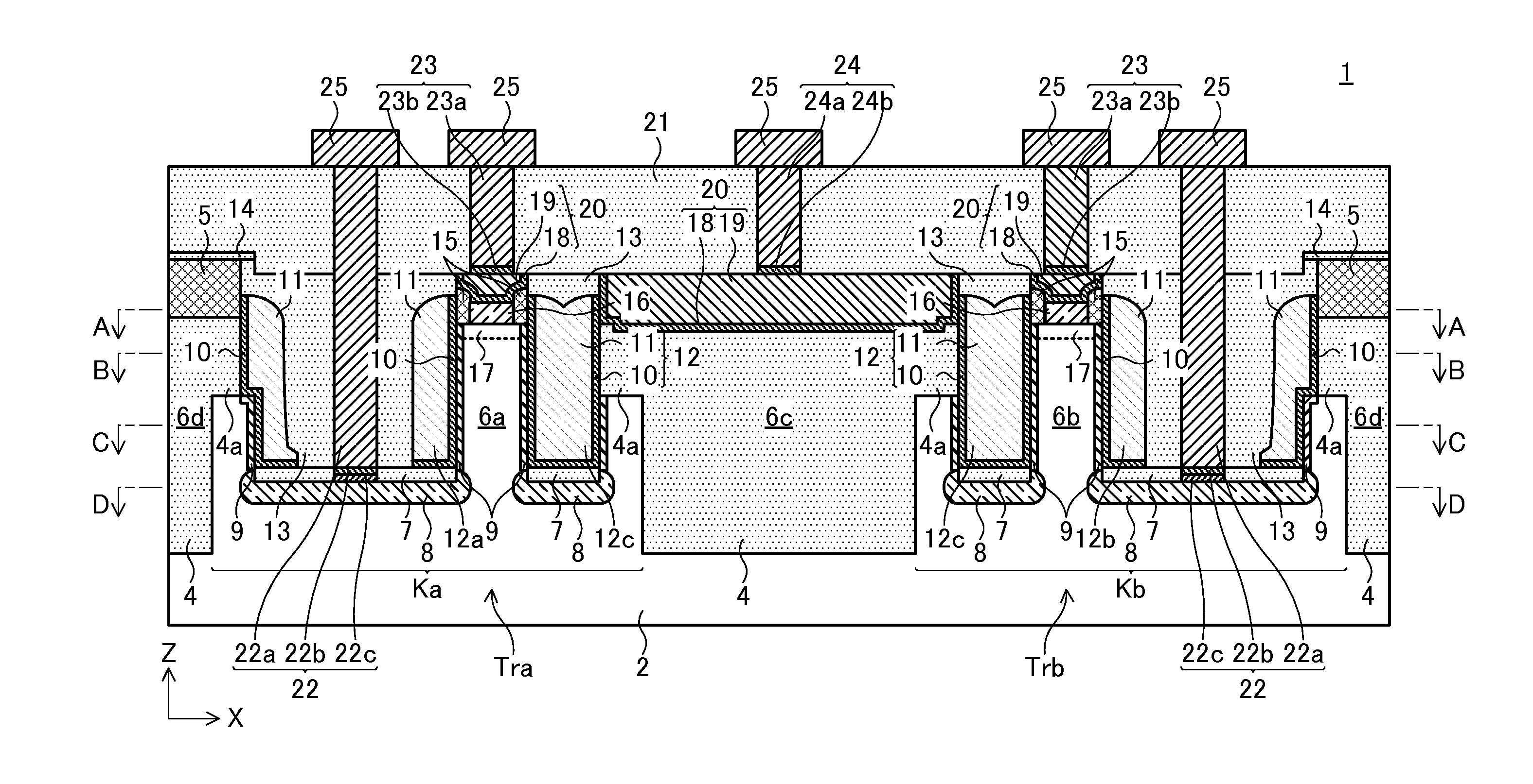
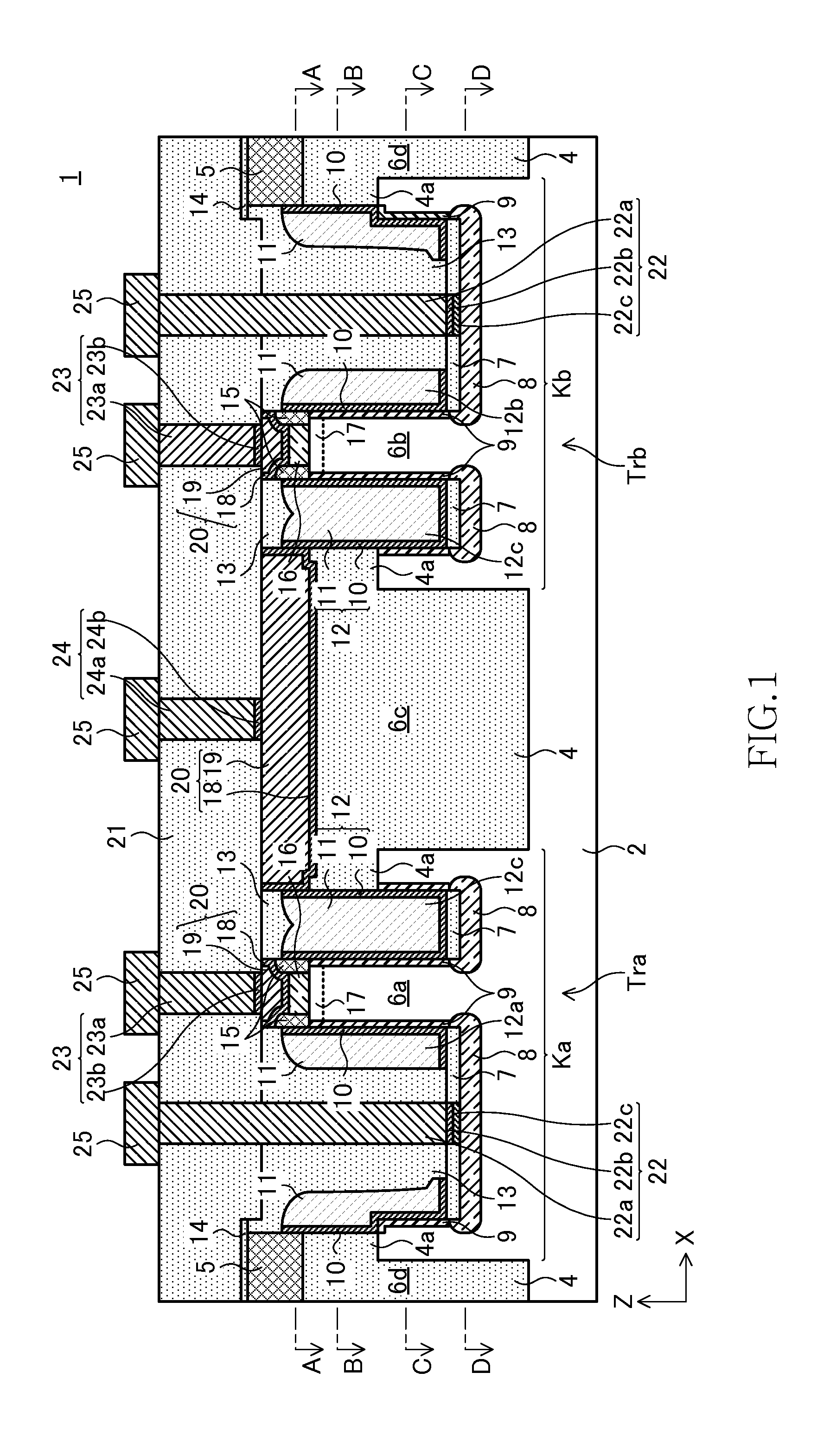
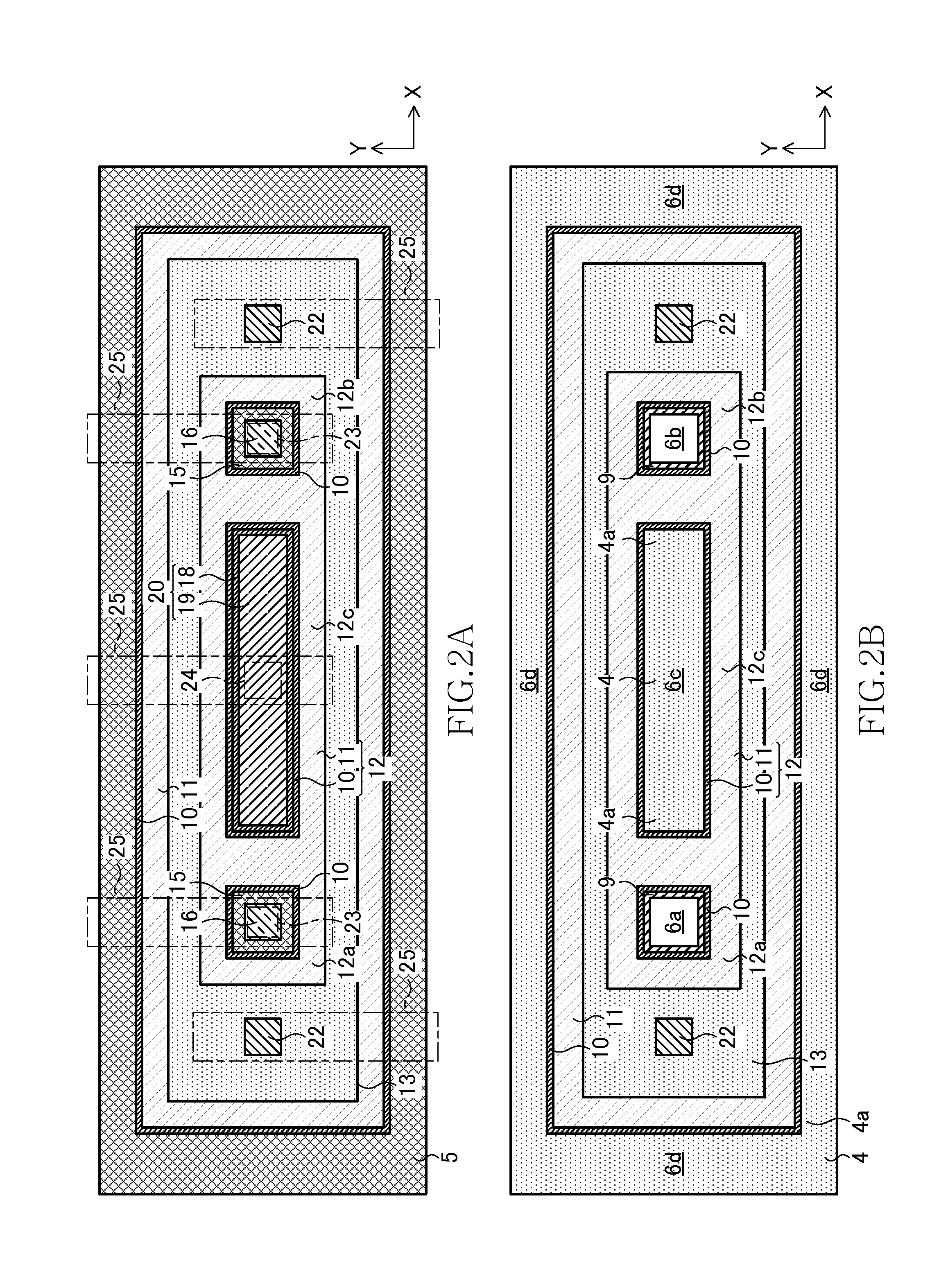
[0019]Referring now to FIGS. 1, 2A, 2B, 3A, and 3B, the semiconductor device 1 according to the present invention includes a semiconductor (silicon) substrate 2. A silicon oxide film 4 constituting element isolation regions according to a shallow trench isolation (STI) method is embedded in the main surface of the semiconductor substrate 2. A first active region Ka and a second active region Kb adjoining each other in an X direction are defined on the main surface of the semiconductor substrate 2 by the silicon oxide film 4. Part of the silicon oxide film 4 (silicon oxide films 4a shown in FIGS. 1 and 2B) is formed to protrude out on the first and second active regions Ka and Kb.
[0020]In the present embodiment, as will be described in detail later, the first and second active regions Ka and Kb each include a vertical transistor (transistor having a channel region formed in a Z direction). Hereinafter, the vertical transistor formed in the first active region Ka will be referred to a...
second embodiment
[0072]FIG. 11 shows a sectional view of the semiconductor device 1 according to the present invention, taken along a plane corresponding to the line A-A of FIG. 1. FIG. 11 also shows a planar arrangement of upper diffusion layer contact plugs 23, gate contact plugs 24, and wiring traces 25-1 to 25-3.
[0073]As shown in FIG. 11, the semiconductor device 1 according to the present embodiment includes transistors Tr1 to Tr6 and the wiring traces 25-1 to 25-3 which connect the transistors Tr1 to Tr6. The transistors Tr1 and Tr2 have the same structure as that of the transistors Tra and Trb described in the first embodiment. Similarly, the transistors Tr3 and Tr4 and the transistors Tr5 and Tr6 both have the same structure as that of the transistors Tra and Trb described in the first embodiment. In the following description, the suffixes “1” to “6” attached to the reference symbols of components represent that the components are ones corresponding to the transistors Tr1 to Tr6, respectivel...
third embodiment
[0081]FIG. 12 shows a sectional view of the semiconductor device 1 according to the present invention, taken along a plane corresponding to the line A-A of FIG. 1. FIG. 12 also shows a planar arrangement of upper diffusion layer contact plugs 23, gate contact plugs 24, and wiring traces 25-1a, 25-1b, 25-2, and 25-3. FIG. 13 shows a sectional view of the semiconductor device 1 according to the present embodiment, taken along a plane corresponding to the line D-D of FIG. 1.
[0082]As shown in FIGS. 12 and 13, the semiconductor device 1 according to the present embodiment includes transistors Tr1 to Tr6 and the wiring traces 25-1a, 25-1b, 25-2, and 25-3 which connect the transistors Tr1 to Tr6. The structures and arrangement of the transistors and the shapes and arrangement of the wiring traces are similar to those described in the second embodiment. Differences lie in that the active regions are made common, that two lower diffusion layer contact plugs 22 are provided for the transistor...
PUM
 Abstract
Description
Claims
Application Information
 - R&D Engineer
- R&D Manager
- IP Professional
- Industry Leading Data Capabilities
- Powerful AI technology
- Patent DNA Extraction
Browse by: Latest US Patents, China's latest patents, Technical Efficacy Thesaurus, Application Domain, Technology Topic.
© 2024 PatSnap. All rights reserved.Legal|Privacy policy|Modern Slavery Act Transparency Statement|Sitemap