Touch panel

a technology of touch panel and input device, applied in the field of touch panel, can solve the problems of inability to smoothly supply, metal electrodes may be visually seen by users, and it is difficult to efficiently operate products using only a keyboard and a mouse currently serving as input devices, etc., to achieve the effect of effectively shielding noise, not excessive capacitance, and reducing the thickness of the member

Inactive Publication Date: 2013-10-24
SAMSUNG ELECTRO MECHANICS CO LTD
View PDF11 Cites 14 Cited by
  • Summary
  • Abstract
  • Description
  • Claims
  • Application Information

AI Technical Summary

Benefits of technology

[0015]The present invention has been made in an effort to provide a touch panel capable of being manufactured to minimize a thickness of members, such as an insulating layer formed between electrode patterns facing each other, and the like, and effectively shielding noises occurring from an image display device, by providing a structure in which capacitance is not excessively largely formed while an electrode pattern has low resistance.

Problems solved by technology

While the rapid advancement of an information-oriented society has widened the use of computers more and more, it is difficult to efficiently operate products using only a keyboard and a mouse currently serving as an input device.
However, the ITO has excellent electric conductivity, but since indium that is a raw material is expensive rare earth metal and is expected to be depleted within about 10 years, cannot be smoothly supplied.
However, there is problem in that the electrodes of metals may be visually seen by users due to opacity of metals.
As such, the touch panel according to the prior art may degrade performance of shielding noises occurring in an image display device.
However, the structure is vulnerable to noises from the image display device due to the sensing electrode directly facing the image display device and therefore, there is a need to use the front electrode layer for shielding noises or has been restrictedly used for the image display device in which an extremely small amount of noise occurs.
However, the dual layer type needs an insulating layer of approximately 100 μm or more so as to secure appropriate capacitance (C) and touch strength (delta C) that can be controlled by a touch IC and therefore, cannot be thinned.
It is impossible to implement the insulating layer having the foregoing thickness only by the current G2 process.

Method used


Image

  • Touch panel
  • Touch panel
  • Touch panel

Examples


Embodiment Construction

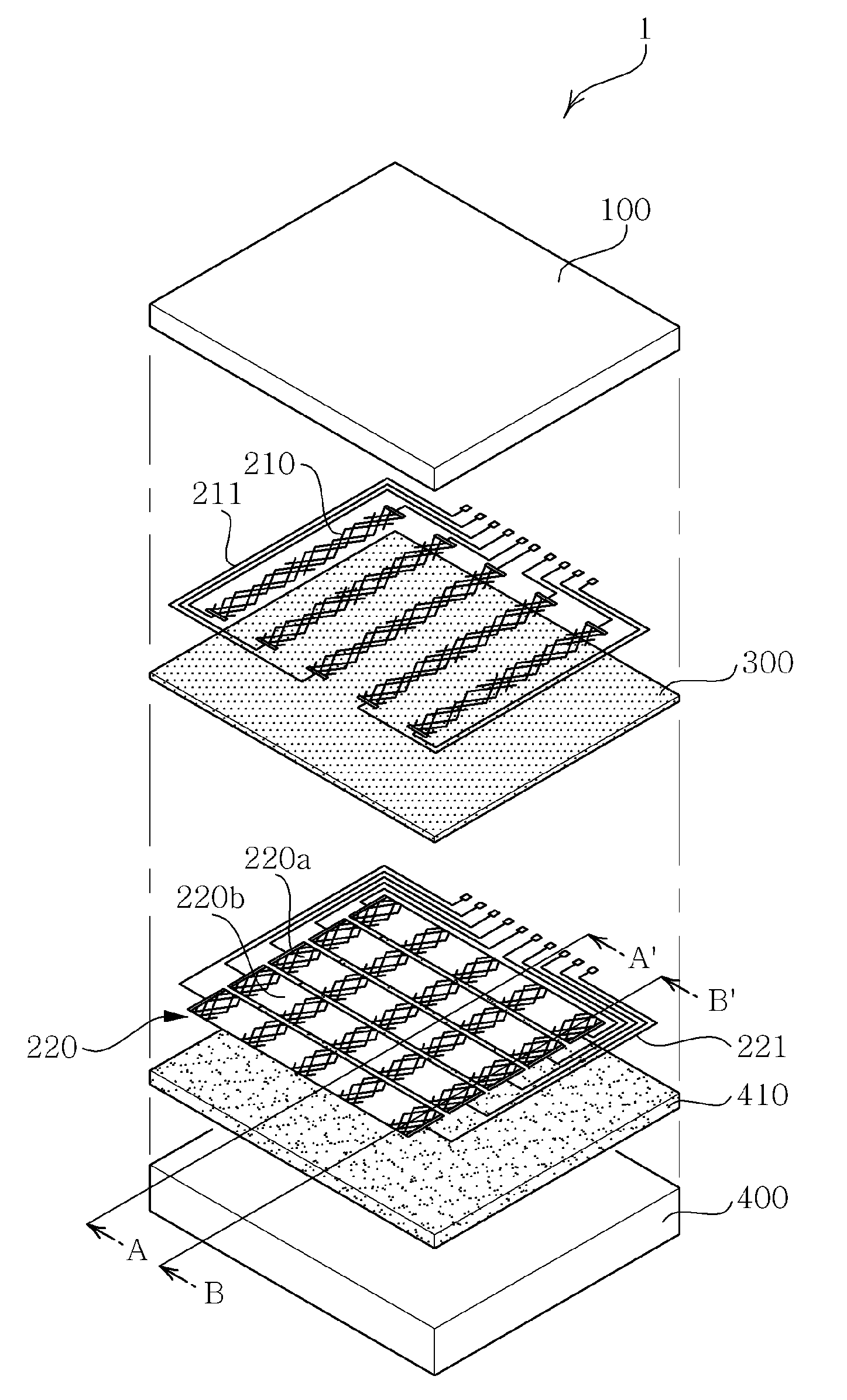
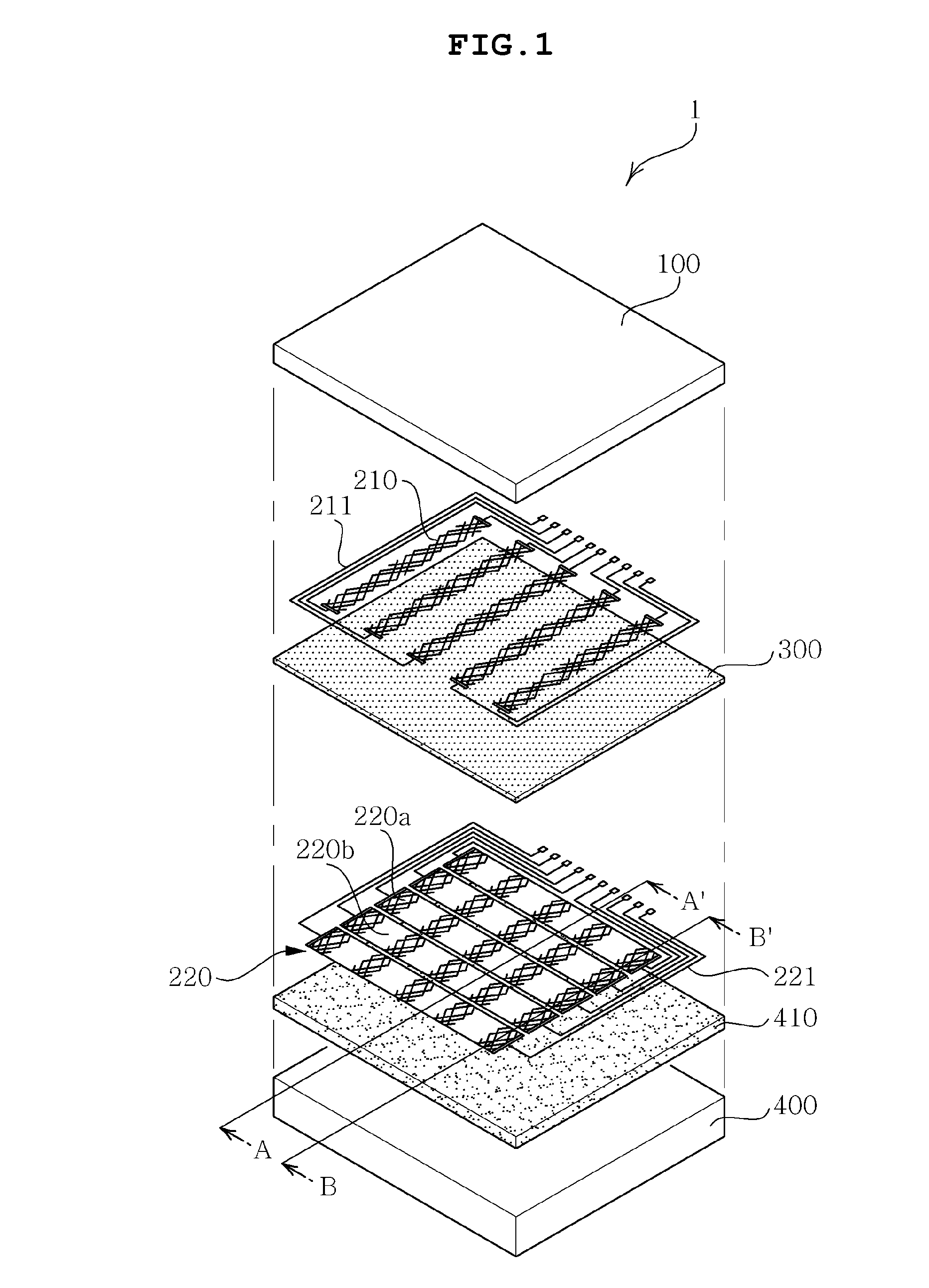
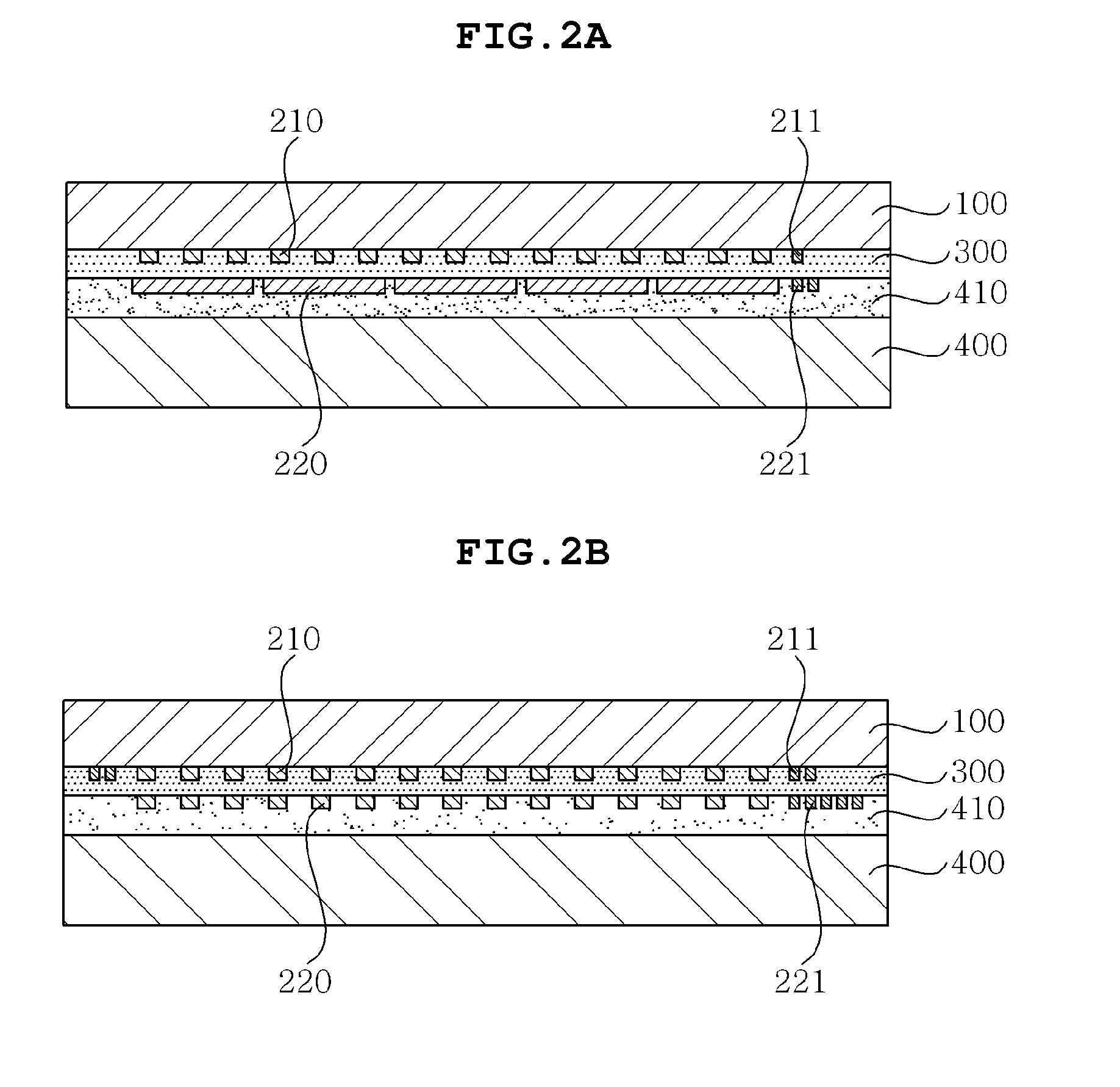
[0041]The objects, features and advantages of the present invention will be more clearly understood from the following detailed description of the preferred embodiments taken in conjunction with the accompanying drawings. Throughout the accompanying drawings, the same reference numerals are used to designate the same or similar components, and redundant descriptions thereof are omitted. Further, in the following description, the terms “first”, “second”, “one side”, “the other side” and the like are used to differentiate a certain component from other components, but the configuration of such components should not be construed to be limited by the terms. Further, in the description of the present invention, when it is determined that the detailed description of the related art would obscure the gist of the present invention, the description thereof will be omitted.

[0042]Hereinafter, preferred embodiments of the present invention will be described in detail with reference to the attac...


PUM

PropertyMeasurementUnit
thicknessaaaaaaaaaa
transparentaaaaaaaaaa
areaaaaaaaaaaa

Abstract

Disclosed herein is a touch panel, including: a transparent substrate; a first electrode pattern formed on the transparent substrate in a mesh pattern; an insulating layer formed on the transparent substrate; and a second electrode pattern formed on an exposed surface of the insulating layer and having an intersecting area facing the first electrode pattern formed in a mesh pattern and an area other than the intersecting area formed in a surface type. By this configuration, even though the thickness of the insulating layer is thinly manufactured, it is possible to secure the desired touch sensitivity and effectively shield noises occurring from an image display device.

Description

CROSS REFERENCE TO RELATED APPLICATION[0001]This application claims the benefit of Korean Patent Application No. 10-2012-0042816, filed on Apr. 24, 2012, entitled “Touch Panel”, which is hereby incorporated by reference in its entirety into this application.BACKGROUND OF THE INVENTION[0002]1. Technical Field[0003]The present invention relates to a touch panel.[0004]2. Description of the Related Art[0005]In accordance with the growth of computers using a digital technology, devices assisting computers have also been developed, and personal computers, portable transmitters and other personal information processors execute processing of text and graphics using a variety of input devices such as a keyboard and a mouse.[0006]While the rapid advancement of an information-oriented society has widened the use of computers more and more, it is difficult to efficiently operate products using only a keyboard and a mouse currently serving as an input device. Therefore, the necessity for a devic...

Claims


Application Information

Patent Timeline
Patent Type & Authority Applications(United States)
IPC IPC(8): H03K17/975G06F3/044
CPCG06F2203/04112G06F2203/04107G06F3/0443G02F1/13338G06F3/044G06F2203/04103
Inventor KIM, HYUN JUNPARK, HO JOON
Owner SAMSUNG ELECTRO MECHANICS CO LTD
Why Eureka
Try Eureka