Laser processing apparatus

a technology of laser processing and laser cutting, which is applied in the direction of manufacturing tools, printed circuit manufacturing, welding/soldering/cutting articles, etc., can solve the problems of difficult to reduce the size of the electrode pad on the printed wiring board to less than 100 m, and the problem of hardly being able to cope, so as to shorten the cycle time for forming the holes, prevent any local concentration of thermal stress, and enhance the positional precision

Active Publication Date: 2013-10-31
V TECH CO LTD
View PDF3 Cites 10 Cited by
  • Summary
  • Abstract
  • Description
  • Claims
  • Application Information

AI Technical Summary

Benefits of technology

[0016]According to a first aspect of the invention, the plurality of predetermined positions on the workpiece can be irradiated with the laser beams by using the micro lens array that can be formed by the photolithography, thereby enhancing the positional precision in the formation of the plurality of holes. Moreover, the plurality of positions on the workpiece can be simultaneously irradiated with the laser beam, thereby shortening the cycle time for forming the holes.
[0017]Furthermore, according to a second aspect of the invention, the uniform intensity distribution of the laser beams can be achieved, so that the holes are formed in the uniform depth.
[0018]Furthermore, according to a third aspect of the invention, the hole having a perfect circular shape can be formed. Consequently, it is possible to prevent any local concentration of a thermal stress caused by the irradiation of the laser beams so as to prevent a crack on the workpiece.

Problems solved by technology

Therefore, when a wiring of 100 μm to 150 μm is to be formed between the electrode terminals on the semiconductor chip, an extra space in the wiring ranges from about 25 μm to about 50 μm, thereby inducing a risk of deficiency such as shorting of wiring.
Moreover, in the above-described conventional laser processing apparatus, the problem of the positional accuracy in boring makes it difficult to reduce the size of the electrode pad on the printed wiring board down to less than 100 μm.
Therefore, when the arrangement pitch between the electrode terminals on the semiconductor chip is less than 300 μm, the problem can be hardly coped with.
Additionally, a plurality of holes are formed by the laser beam while the galvano scanner repetitively moves the laser beam irradiation position, thereby raising a problem of a long cycle time for forming a plurality of holes.

Method used


Image

  • Laser processing apparatus
  • Laser processing apparatus
  • Laser processing apparatus

Examples


Embodiment Construction

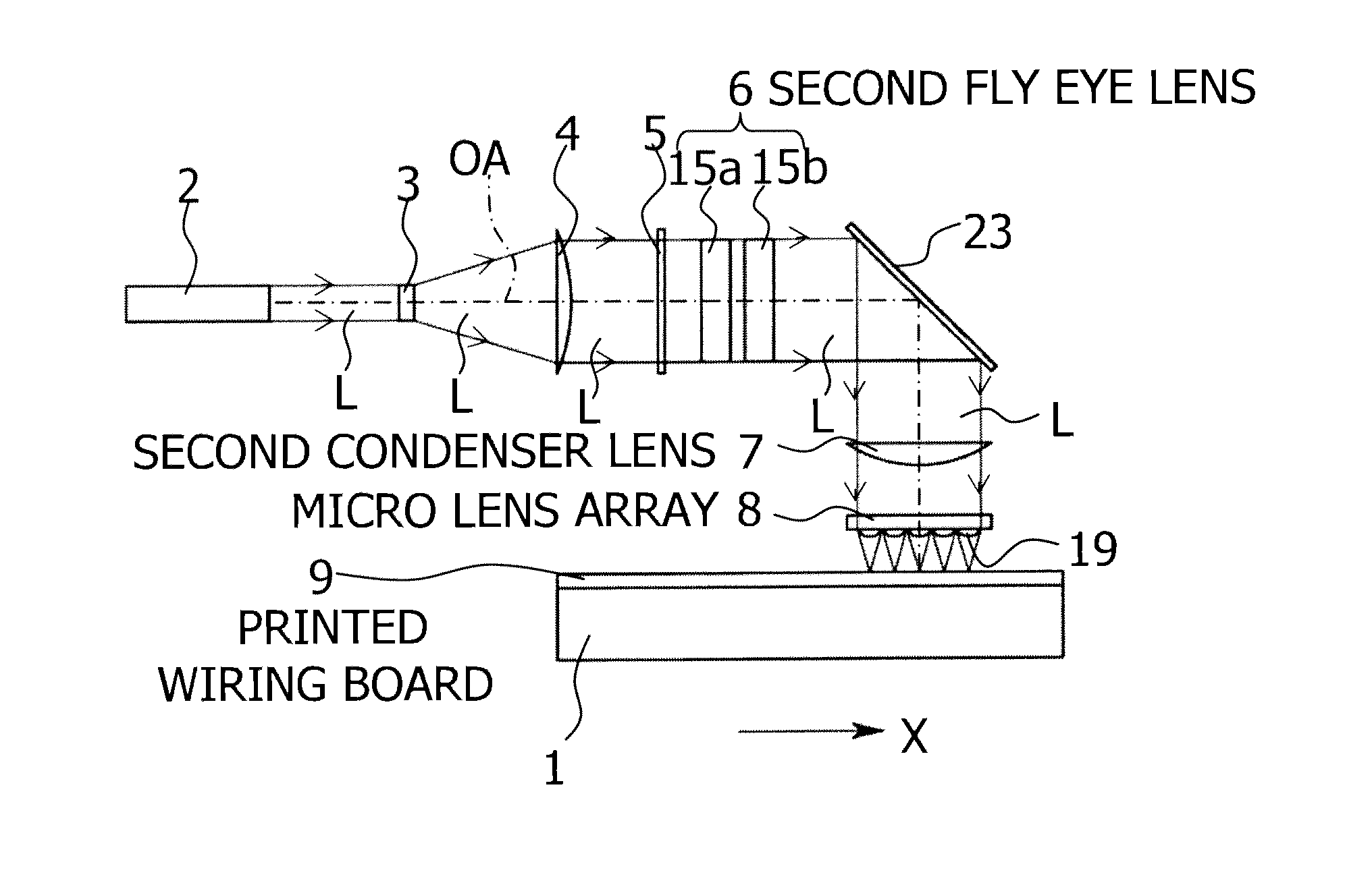
[0024]A description will be given below in detail of an embodiment according to the present invention with reference to the attached drawings. FIG. 1 is a front view showing a laser processing apparatus in an embodiment according to the present invention. The laser processing apparatus is adapted to irradiate a workpiece with a laser beam and form holes at a plurality of predetermined positions on the workpiece. The laser processing apparatus includes an XY stage 1, a laser beam source 2, a first fly eye lens 3, a first condenser lens 4, a diffusing plate 5, a second fly eye lens 6, a second condenser lens 7, and a micro lens array 8.

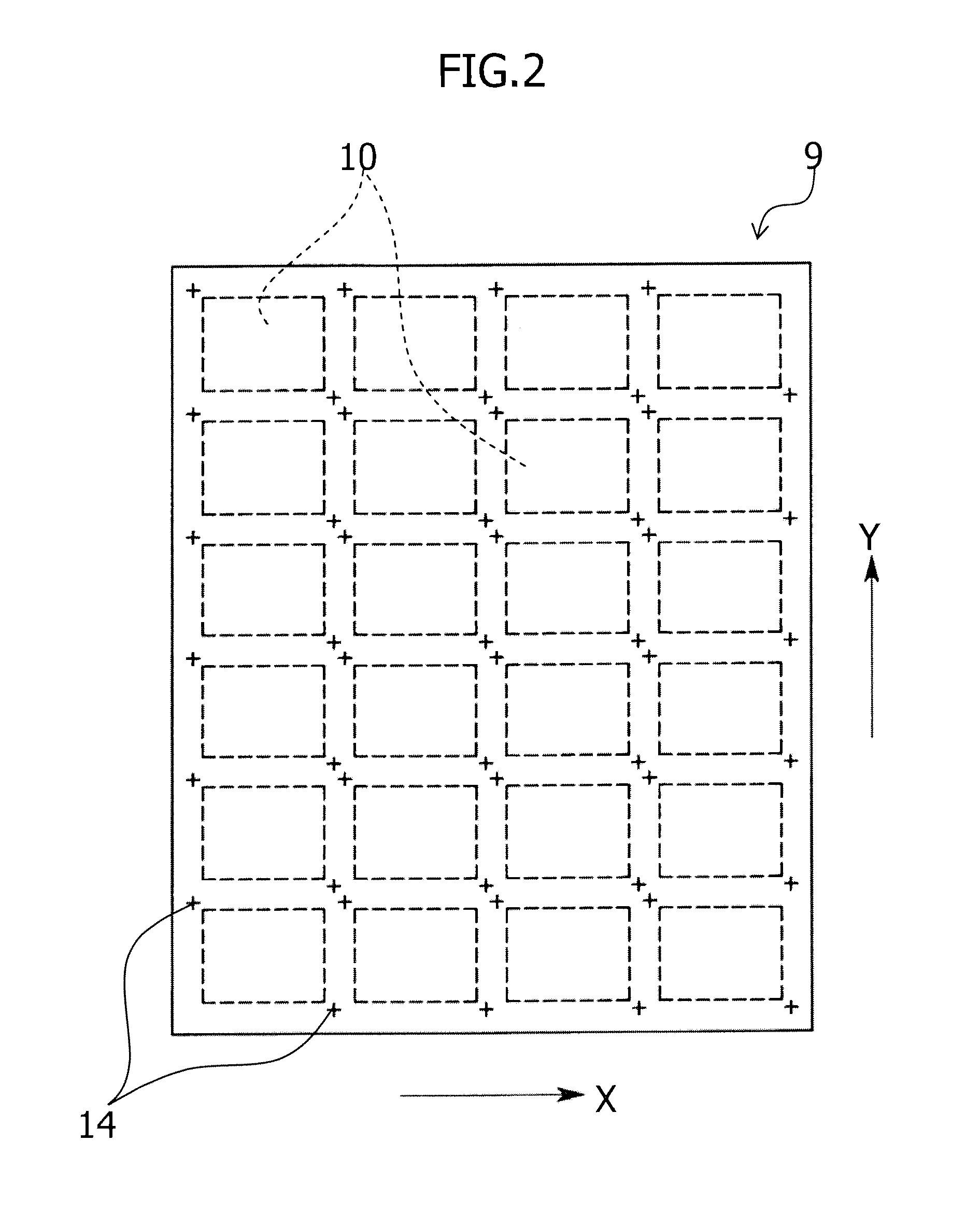
[0025]The XY stage 1 is adapted to positionally mount thereon a workpiece such as a printed wiring board 9, and further, to move it within an XY two-dimensional plane. The XY stage 1 includes position sensors on an X-axis and a Y-axis, which are not shown. Moreover, the XY stage 1 is designed to be freely turned by a predetermined angle around the cente...


PUM

PropertyMeasurementUnit
diameteraaaaaaaaaa
sizeaaaaaaaaaa
wavelengthaaaaaaaaaa

Abstract

The present invention relates to a laser processing apparatus for irradiating a printed wiring board 9 with a laser beam L so as to form holes 22 at a plurality of predetermined positions on the printed wiring board 9. The device includes, from upstream on an optical path of the laser beam: a second fly eye lens 6 that achieves the uniform intensity distribution of the laser beam L; a second condenser lens 7 that collimates the laser beam L emitted from the second fly eye lens 6; and a micro lens array 8 positioned in a manner facing the printed wiring board 9 and having a plurality of micro lenses 19 formed in a manner corresponding to the plurality of positions on the printed wiring board 9.

Description

[0001]This application is a continuation of PCT / JP2011 / 059436, filed on Apr. 15, 2011.BACKGROUND OF THE INVENTION[0002]1. Field of the Invention[0003]The present invention relates to a laser processing apparatus for irradiating a workpiece with a laser beam so as to bore the workpiece at a plurality of predetermined positions and, more particularly, a laser processing apparatus that intends to enhance the positional accuracy in forming a plurality of holes and shorten a cycle time for boring.[0004]2. Description of Related Art[0005]In a conventional laser processing apparatus, a galvano scanner guides a laser beam to an irradiation position on a workpiece, and then, irradiates the workpiece at the laser beam irradiation position, at which holes are formed, with a pulsed laser beam by burst shooting. Two galvano scanners that are orthogonally and biaxially oscillated are respectively oscillated at a high speed, thereby moving the laser beam irradiation position so as to locate it at ...

Claims


Application Information

Patent Timeline
Patent Type & Authority Applications(United States)
IPC IPC(8): B23K26/38B23K26/067B23K26/064B23K26/382H05K3/00
CPCB23K26/0676B23K26/4025B23K26/4075B23K26/381B23K26/382B23K26/40B23K2103/50B23K26/38B23K26/064B23K26/067B23K26/402
Inventor MIZUMURA, MICHINOBU
Owner V TECH CO LTD
Why Eureka
Try Eureka