Radiological image detection apparatus and method of manufacturing the same
a technology of radiological image and detection apparatus, which is applied in the direction of radiation intensity measurement, x/gamma/cosmic radiation measurement, instruments, etc., can solve the problems of insufficient sensitivity and image blur, and achieve high light emission efficiency of fluorescence, improve the amount of light incident, and improve the effect of crystallinity
- Summary
- Abstract
- Description
- Claims
- Application Information
AI Technical Summary
Benefits of technology
Problems solved by technology
Method used
Image

Examples
manufacturing example 1
[0170]1. Film-Forming of Scintillator
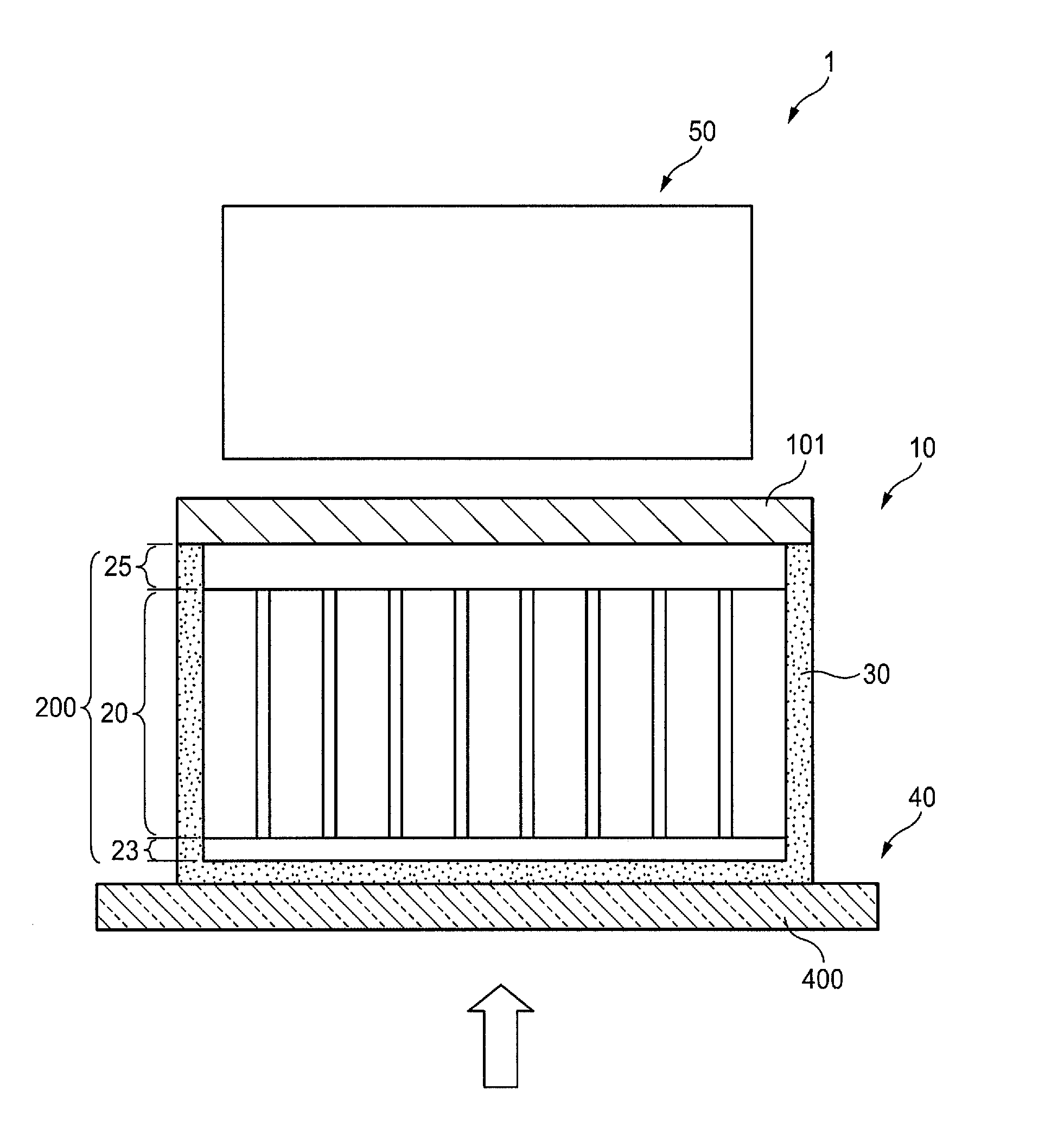
[0171]An alkali-free glass substrate (0.7 mm) for liquid crystals was prepared as the support.
[0172]First, surface treatment was performed to the support for the purpose of improving the adhesion with the CsI crystal layer. Then, the surface treated support was set in a vacuum chamber for scintillator film-forming. The vacuum chamber was provided with a plurality of crucibles for independently heating each of the CsI and Tl which are the raw materials of the vacuum chamber. After evacuating the chamber, a predetermined amount of Ar was introduced, thereby setting the degree of vacuum of the device to 0.75 Pa. At the time when the molten state of the raw materials was stabilized by heating the raw material crucibles, the support was concentrically rotated by a device instrument of a vacuum device and a shutter was opened, thereby starting the deposition of the second non-columnar section.
[0173]Film fabrication was performed at these conditions. Wh...
manufacturing example 12
[0195]The substrate was changed to the glass substrate used in manufacturing example 1 as the support. The glass substrate was formed with unevenness through wet etching with an about 5 μm pitch and an about 5 μm height on the surface of the glass substrate and used.
[0196]In forming the scintillator, the radiological image detection apparatus of Manufacturing Example 12 was manufactured as in Manufacturing Example 1 except that the columnar crystal layer was directly vapor-deposited on the support without performing the vapor deposition of the non-columnar crystal section. Evaluation was made in the same manner with that of Manufacturing Example 1, and relative evaluation was made assuming the result of Manufacturing Example 12 is 100.
manufacturing examples 2 to 6
[0197]Radiological image detection apparatuses of Fabrication Examples 2 to 6 were manufactured as in Manufacturing Example 1 except that the film thicknesses of the non-columnar crystal sections were adjusted as represented in Table 1 by changing the deposition time when the degree of vacuum was 0.75 Pa, and evaluated in the same manner. The results are represented in Table 1 below.
PUM
 Abstract
Description
Claims
Application Information