Optical-electrical composite flexible circuit substrate
a technology of optical fiber cables and flexible circuits, applied in the direction of circuit optical details, optical elements, instruments, etc., can solve the problems of optical fiber cables that are difficult to realize, and achieve the effect of high bending resistan
- Summary
- Abstract
- Description
- Claims
- Application Information
AI Technical Summary
Benefits of technology
Problems solved by technology
Method used
Image

Examples
example 1
Practical Example 1
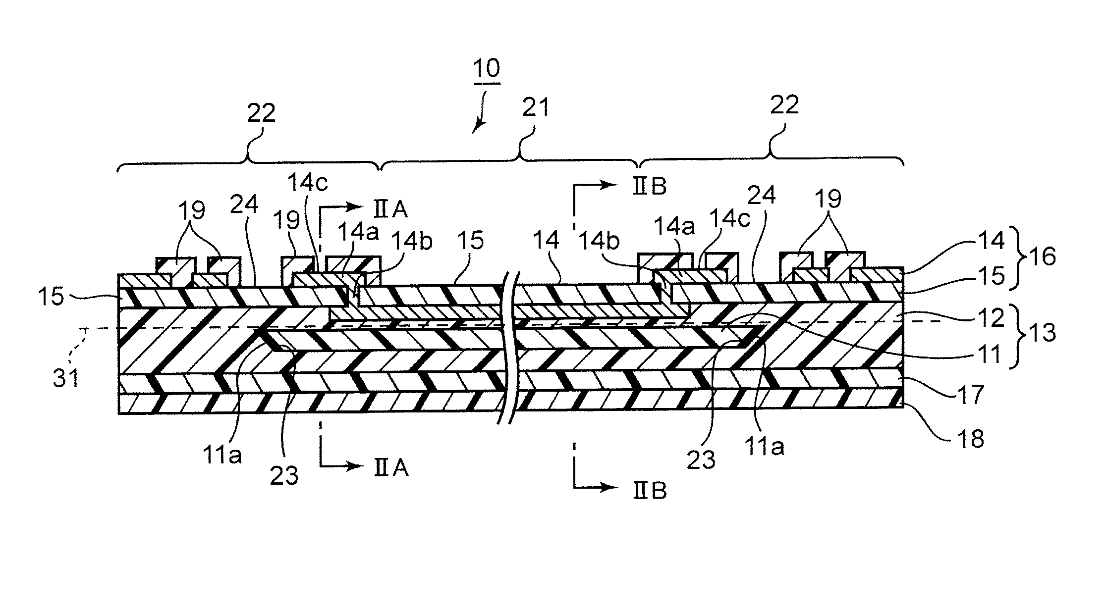
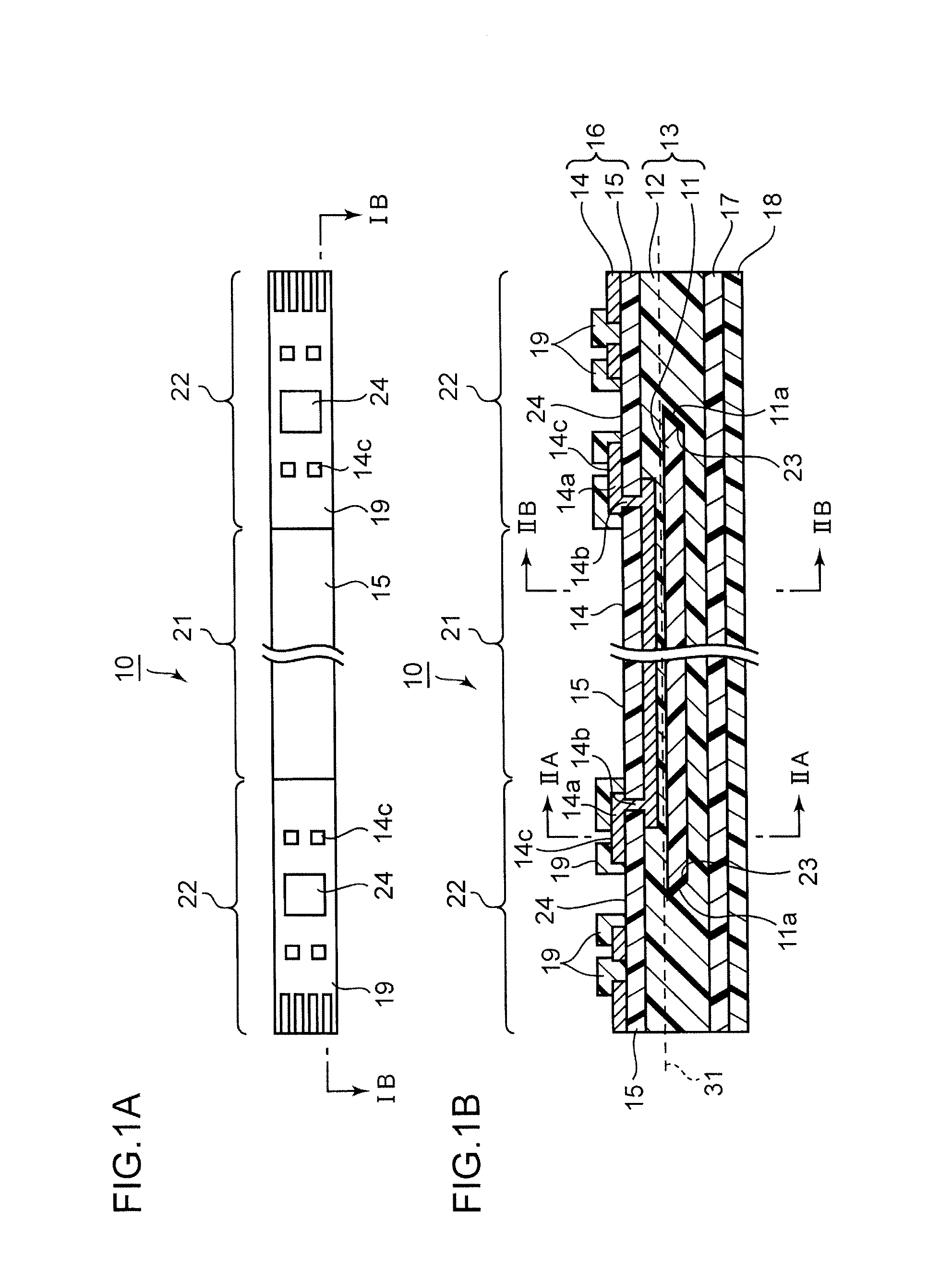
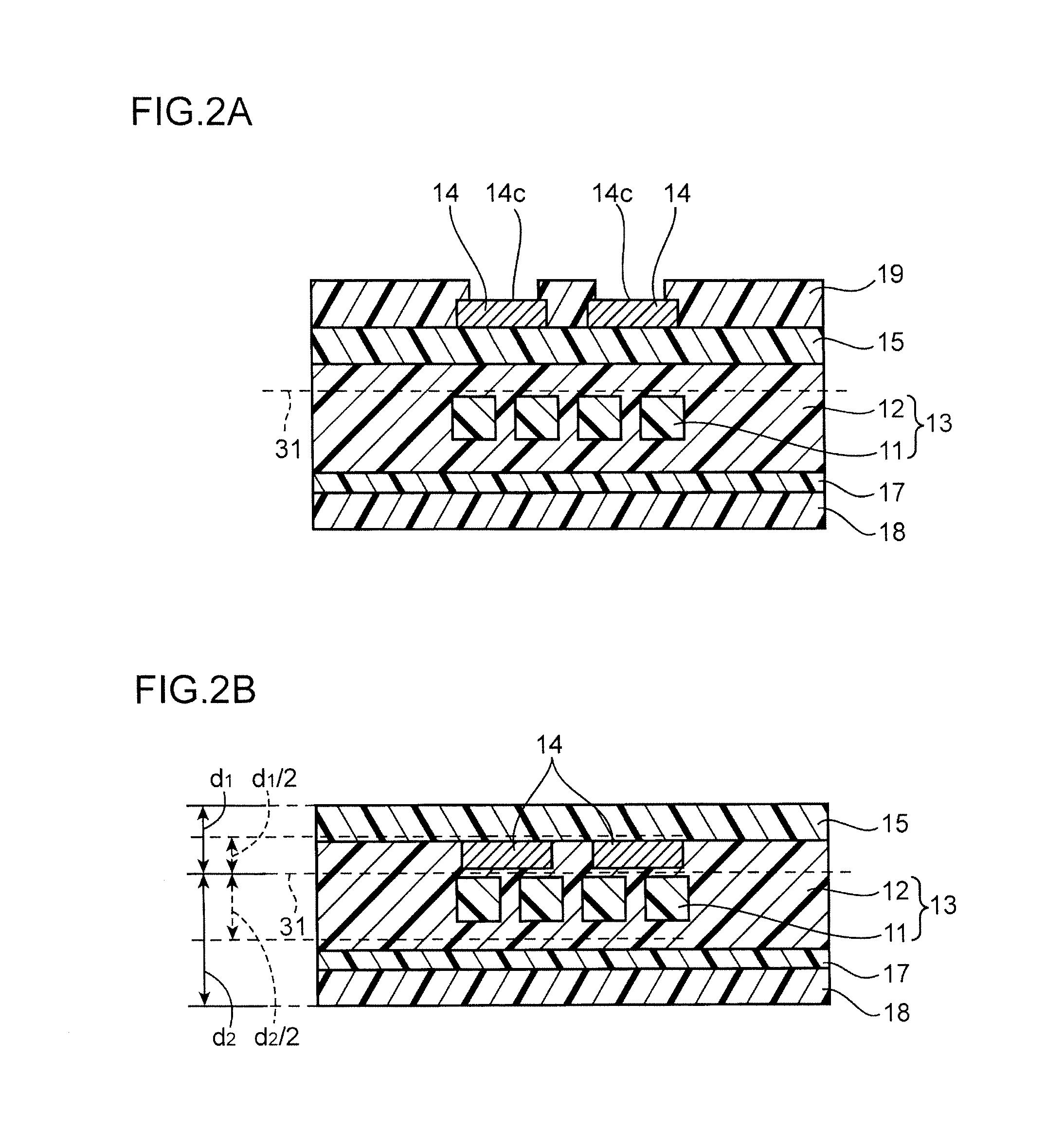
[0137]The optical-electrical composite flexible circuit substrate shown in FIGS. 1A, 1B, 2A, and 2B was manufactured according to the manufacturing method shown in FIGS. 13A to 13I using the respective materials.
[0138]Specifically, the optical-electrical composite flexible circuit substrate was manufactured in the following manner.
[0139]First, a flexible printed wiring substrate (double-sided substrate) having an external size of 130 mm by 130 mm was obtained using a flexible double-sided copper-clad laminated substrate (FELIOS (R-F775), product of Panasonic Electric Works Co., Ltd.) in which a copper foil having a thickness of 12 μm is laminated on both sides of a polyimide film having a thickness of 20 μm. Twenty final product shapes (hereinafter also referred to as “individual pieces”) were arranged at a pitch of 4 mm (center-to-center distance: 4 mm). A schematic shape of each individual piece schematically is shown in FIGS. 12A to 12C. The individual piece ha...
example 2
Practical Example 2
[0150]The optical-electrical composite flexible circuit substrate shown in FIGS. 7A and 7B was manufactured according to the manufacturing method shown in FIGS. 14A to 14L using the respective materials.
[0151]The other conditions were the same as those of Practical Example 1 except for the following differences.
[0152]As a first difference, when the first cladding layer was formed, the first cladding layer resin film was irradiated with ultraviolet light so that the first cladding layer had the shape as shown in FIG. 14C.
[0153]As a second difference, when the second cladding layer was formed, the second cladding layer resin film was irradiated with ultraviolet light so that the second cladding layer has the shape as shown in FIG. 14I.
[0154]As a third difference, the coverlay layer was formed so as to cover the optical circuit using a coverlay film having a thick adhesive layer as shown in FIG. 14K. Specifically, a halogen-free coverlay film R-CAES (product of Panas...
example 3
Practical Example 3
[0156]The optical-electrical composite flexible circuit substrate shown in FIGS. 8A, 8B, 9A, and 9B was manufactured according to the manufacturing method shown in FIGS. 16A to 16I using the respective materials.
[0157]Specifically, the optical-electrical composite flexible circuit substrate was manufactured in the following manner.
[0158]First, a flexible printed wiring substrate (double-sided substrate) having an external size of 130 mm by 130 mm was obtained using a flexible double-sided copper-clad laminated substrate (FELIOS (R-F775), product of Panasonic Electric Works Co., Ltd.) in which a copper foil having a thickness of 12 μm is laminated on both sides of a polyimide film having a thickness of 20 μm. Twenty final product shapes (hereinafter also referred to as “individual pieces”) were arranged at a pitch of 4 mm (center-to-center distance: 4 mm). A schematic shape of each individual piece schematically is shown in FIGS. 15A to 15C. The individual piece ha...
PUM
 Abstract
Description
Claims
Application Information
 - Generate Ideas
- Intellectual Property
- Life Sciences
- Materials
- Tech Scout
- Unparalleled Data Quality
- Higher Quality Content
- 60% Fewer Hallucinations
Browse by: Latest US Patents, China's latest patents, Technical Efficacy Thesaurus, Application Domain, Technology Topic, Popular Technical Reports.
© 2025 PatSnap. All rights reserved.Legal|Privacy policy|Modern Slavery Act Transparency Statement|Sitemap|About US| Contact US: help@patsnap.com