Leadframe having selective planishing

a technology of leadframe and planishing, which is applied in the direction of electrical apparatus construction details, casings/cabinets/drawers, casings/cabinets/drawers details, etc., can solve the problem of leadframe deformation, more difficult to maintain mold compound adhesion to leadframes, and yield losses of approximately 5%, etc. problem, to achieve the effect of reducing manufacturing cost, increasing insensitivity, and reducing production costs

Active Publication Date: 2013-11-07
TEXAS INSTR INC
View PDF26 Cites 8 Cited by
  • Summary
  • Abstract
  • Description
  • Claims
  • Application Information

AI Technical Summary

Benefits of technology

[0009]Among dominating market trends for semiconductor products are the demand for increased insensitivity against temperature variations and moisture level exposure, and the need to keep fabrication cost down by employing inexpensive process steps. For semiconductor packages, the first trend implies an increased need for creating reliable adhesion between the different package parts and maintaining the adhesion through mechanically rough process steps, such as degating, deflashing, and trimming and forming. The second trend implies a necessity to avoid expensive process techniques such as selective plating and to select inexpensive process steps throughout such as flood plating.
[0012]In a careful failure analysis, applicant discovered as the root cause of the leadframe deformation the enhanced adhesion between the roughened leadframe surfaces and the molding compound in zones such as the mold runners where the plastic crosses the leadframe strip outside the package.

Problems solved by technology

In addition, the requirement to use lead-free solders pushes the reflow temperature range into the neighborhood of about 260° C., making it more difficult to maintain mold compound adhesion to the leadframes.
Analyzing quality and productivity issues of molded plastic devices, applicant observed that the process steps of degating after molding frequently causes deformation of the leadframe during the gate removal step.
As a consequence of this deformation, yield losses of approximately 5% may occur at the process step of trimming-and-forming.

Method used


Image

  • Leadframe having selective planishing
  • Leadframe having selective planishing
  • Leadframe having selective planishing

Examples


Embodiment Construction

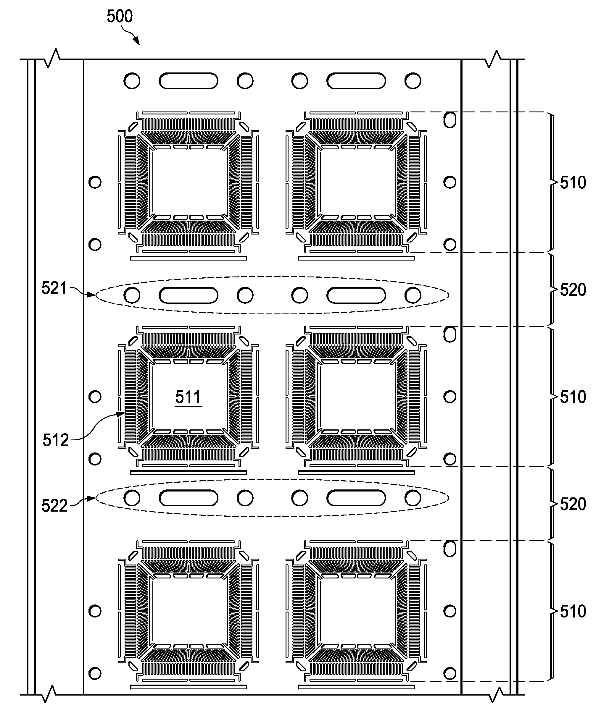
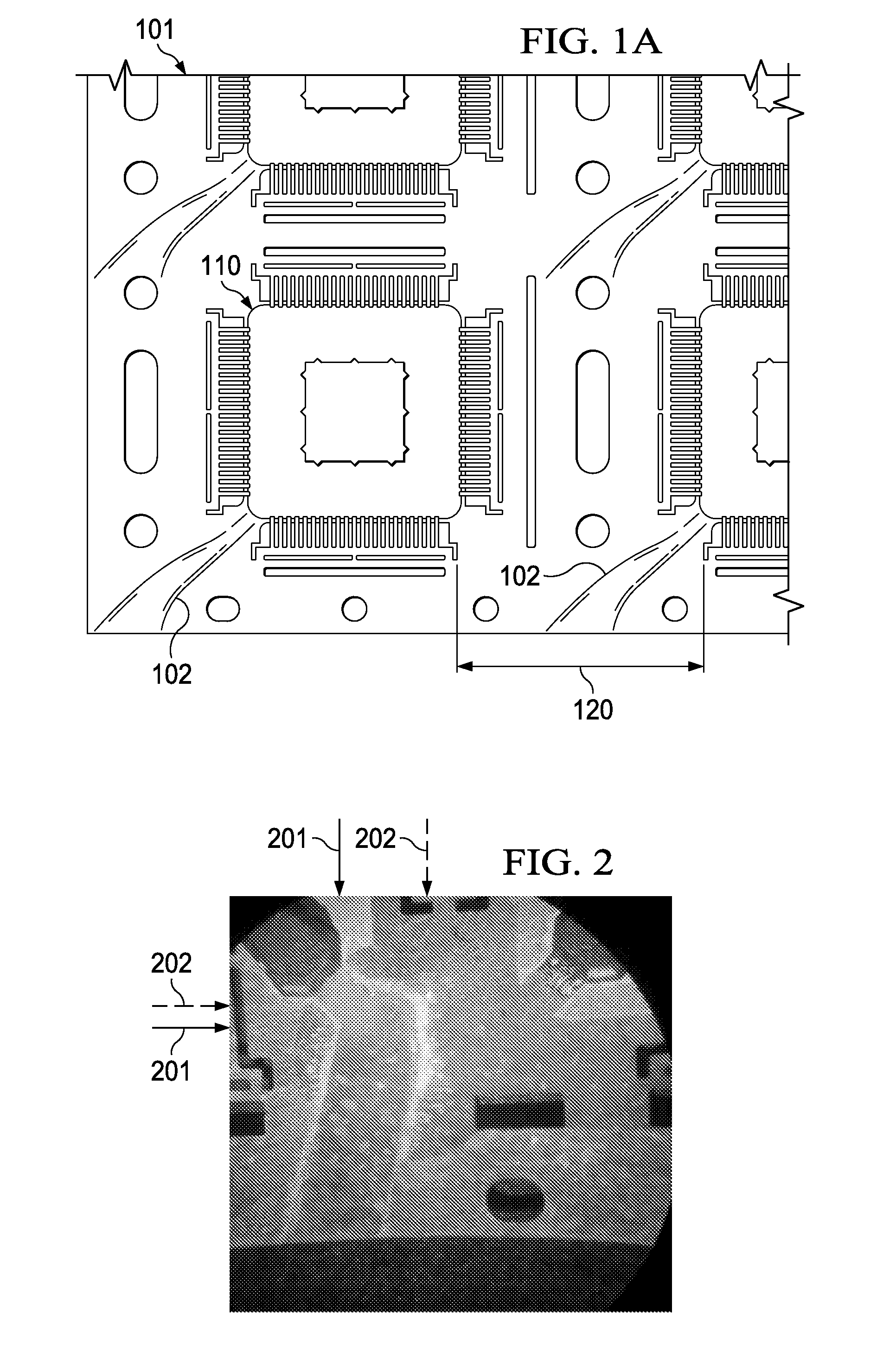
[0027]FIG. 1A illustrates a portion of an exemplary leadframe strip 101 with molded semiconductor devices 110 after the strip has been removed from the mold press, in which the encapsulation process by molding had been completed. A leadframe strip is preferably etched or stamped from a thin sheet of base metal such as copper, copper alloy, iron-nickel alloy, aluminum, Kovar™, and others, in a typical thickness range from 120 to 250 μm. The technology trend is towards thinner leadframes. As used herein, the term base metal has the connotation of starting material and does not imply a chemical characteristic.

[0028]A leadframe provides a stable support pad for firmly positioning the semiconductor chip. Further, a leadframe offers a multitude of conductive leads to bring various electrical conductors into close proximity of the chip. Any remaining gap between the tip of the leads and the chip terminals is typically bridged by thin bonding wires; alternatively, in flip-chip technology th...


PUM

PropertyMeasurementUnit
roughnessaaaaaaaaaa
roughnessaaaaaaaaaa
roughnessaaaaaaaaaa

Abstract

A metal leadframe strip (500) for semiconductor devices is described. The leadframe strip has a plurality of sites (510) for assembling semiconductor chips. The sites alternate with zones (520) for connecting the leadframe to molding compound runners. The sites (510) have mechanically rough and optically matte surfaces (511, 512). The zones (520) have at least portions with mechanically flattened and optically shiny metal surfaces (521, 522). The flattened surface portions transition into the rough surface portions by a step.

Description

FIELD OF THE INVENTION[0001]The present invention is related in general to the field of semiconductor devices and processes, and more specifically to the structure and fabrication process of flood-plated rough metallic leadframes in semiconductor packages having selectively planished portions to reduce the leadframe adhesion to molding compound in zones exposed to compound in mold runners.DESCRIPTION OF RELATED ART[0002]Based on their functions, semiconductor packages include a variety of different materials. Metals formed as leadframes and bonds are employed for mechanical stability and electrical and thermal conductance, and insulators, such as polymeric molding compounds, are used for encapsulations and form factors. In the packaging fabrication flow, it is common practice to attach a plurality of semiconductor chips to a strip of leadframe, to connect the chips to their respective leads, and then to encapsulate the assembled chips in packages, which protect the enclosed parts ag...

Claims


Application Information

Patent Timeline
Patent Type & Authority Applications(United States)
IPC IPC(8): H01L23/495H01L21/64H05K7/18
CPCH01L23/49541H01L23/49548H01L23/49565H01L2924/0002H01L2924/181H01L2224/85H01L2924/00014H01L21/4821Y10T29/49121H01L2924/00H01L2224/45099H01L2224/05599H01L21/64H01L23/49503H01L23/49575H01L21/4842H01L21/561H01L24/85H01L24/97H01L2924/2064
Inventor ABBOTT, DONALD C.
Owner TEXAS INSTR INC
Why Eureka
Try Eureka