

Superjunction device
a superjunction device and superjunction technology, applied in the direction of semiconductor devices, basic electric elements, electrical apparatus, etc., can solve the problems of the most difficult filling of silicon in the annular trenches, the step of filling the annular trenches is a great challenge, and the design of floating rings and field plates that has been adopted in vertical double-diffused metal-oxide semiconductor (vdmos) transistors is not applicable to conventional superjunction devices
- Summary
- Abstract
- Description
- Claims
- Application Information
AI Technical Summary
Benefits of technology
Problems solved by technology
Method used
Image

Examples
Embodiment Construction
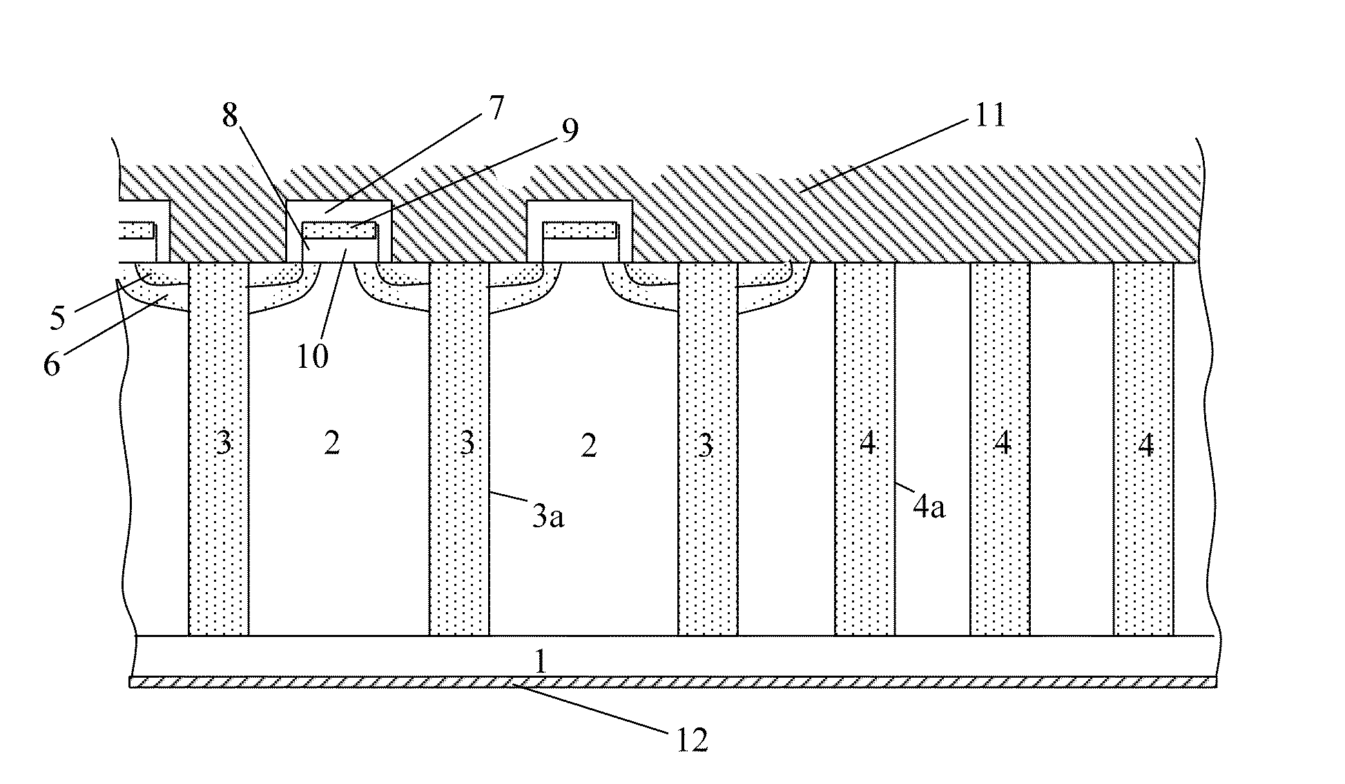
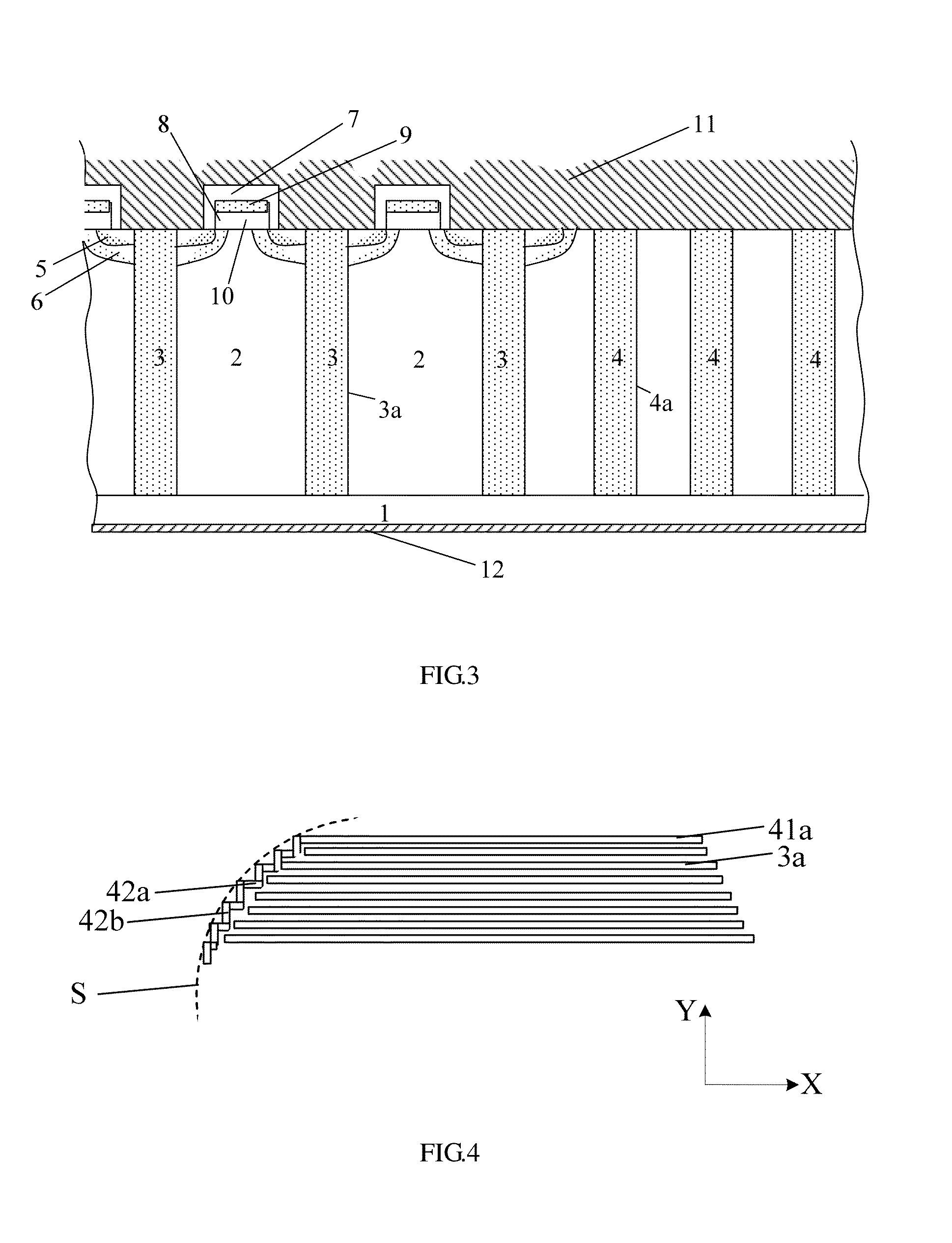
[0025]FIG. 3 is a cross-sectional view of a superjunction device according to the present invention, while FIG. 4 is a top view schematically illustrating a corner portion of the superjunction device according to the present invention. In one embodiment, the superjunction device is an N-channel superjunction MOSFET device.
[0026]In the embodiment, the superjunction device includes an N-type semiconductor substrate 1, which may be a silicon substrate doped with arsenic (As) or antimony (Sb) having a resistivity of 0.001 Ω·cm to 0.009 Ω cm.
[0027]Moreover, the superjunction device further includes an N-type semiconductor epitaxial layer 2 formed on the N-type semiconductor substrate 1. The semiconductor epitaxial layer 2 may be a silicon epitaxial layer which is doped with phosphorus and has a resistivity of 1 Ω·cm to 10 Ω·cm.
[0028]Further, a current-flowing area and a termination structure are formed in the semiconductor epitaxial layer 2.
[0029]The current-flowing area includes a plura...
PUM
 Abstract
Description
Claims
Application Information