Method for Producing a Light-Emitting Semiconductor Component and Light-Emitting Semiconductor Component

a technology of light-emitting semiconductors and semiconductor components, which is applied in the direction of semiconductor/solid-state device manufacturing, semiconductor devices, electrical devices, etc., can solve the problems of inability to optimize chip design and packaging for maximum efficiency, and the protection of light-emitting diodes is not completely clear. , to achieve the effect of reducing the absorption of light, increasing the efficiency of emitted light, and increasing stability

Inactive Publication Date: 2013-11-28
OSRAM OPTO SEMICONDUCTORS GMBH
View PDF23 Cites 19 Cited by
  • Summary
  • Abstract
  • Description
  • Claims
  • Application Information

AI Technical Summary

Benefits of technology

[0039]In comparison with known packages comprising light-emitting diode chips, the semiconductor component described here can have an increased stability even in a moist environment or in an environment having other harmful substances, for example, outdoors since, by means of the encapsulation layer, the semiconductor chip and also the sensitive components such as, for instance, leadframes or conductor tracks, can be protected by the encapsulation layer. Furthermore, it may be possible that, in comparison with known packages, an increase in the efficiency of the emitted light can be achieved since, for example, silver can be used as material for a minor layer and / or for a leadframe and / or for conductor tracks, as a result of which an absorption of light can be considerably reduced in comparison with customary leadframe materials. The susceptibility of silver to migration in particular in a moist or other harmful environment can be prevented in this case by arrangement below the encapsulation layer. Consequently, the semiconductor component described here, in comparison with known packages, can have a generally increased durability and resistance to storage or operating conditions, even in a moist environment and / or in a salt-containing atmosphere and / or in a pollutant-gas-containing atmosphere, for example, a hydrogen sulfide atmosphere.
[0040]In comparison with known packages, the semiconductor component described here can have an increased design freedom in optimizing efficiency since known protective layers, which often absorb light, can be avoided, with the result that a higher luminous efficiency can be produced. Since the semiconductor chip is protected against the environment by the encapsulation layer, the chip design can be simplified, which makes it possible to avoid process costs and an increase in yield by reduction of yield-critical process steps which are necessary in the case of known packages in order to provide the chip with moisture barriers.
[0041]By applying the encapsulation layer, protection of the sensitive regions, for example, regions of the semiconductor chip and / or of the further sensitive materials, element and / or structural parts mentioned above, can be achieved in a single method step, as a result of which a cost saving can be brought about.
[0042]In comparison with known methods, adverse influences, for example, caused by processes such as laser separation for singulating light-emitting diode chips, can be minimized. Light-emitting diode chips are generally characterized a hundred percent in the wafer assemblage before the chips are singulated. Influences resulting from the separating process are not taken into account in this prior measurement. However, separating processes and handling of light-emitting diode chips can cause microscopic hairline cracks in an individual layer or passivation layers of the chips, which can lead to degradation or even to failure of components, because sensitive constituent parts are attacked, only as a result of relatively long operation in a corresponding, in particular moist, environment. Such microscopic damage cannot be detected, but can be effectively closed and thus rendered harmless by means of the encapsulation layer described herein.

Problems solved by technology

In such packages, however, the light-emitting diode chips are not completely protected against harmful substances such as, for instance, moisture or in an environment comprising corrosive or otherwise harmful substances such as, for instance, H2S, SO2 and chlorine.
These requirements have the effect, inter alia, that chip design and packages cannot be optimized for maximum efficiency, because for example light-absorbing moisture barriers have to be incorporated in the light-emitting diode chips and / or in the package for example highly reflective leadframe materials sensitive to moisture or other harmful substances can be used only to a limited extent or even cannot be used at all.

Method used


Image

  • Method for Producing a Light-Emitting Semiconductor Component and Light-Emitting Semiconductor Component
  • Method for Producing a Light-Emitting Semiconductor Component and Light-Emitting Semiconductor Component
  • Method for Producing a Light-Emitting Semiconductor Component and Light-Emitting Semiconductor Component

Examples


Embodiment Construction

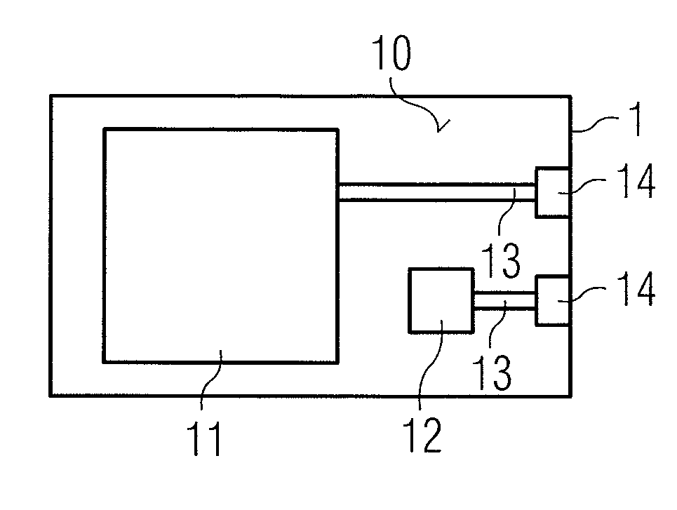
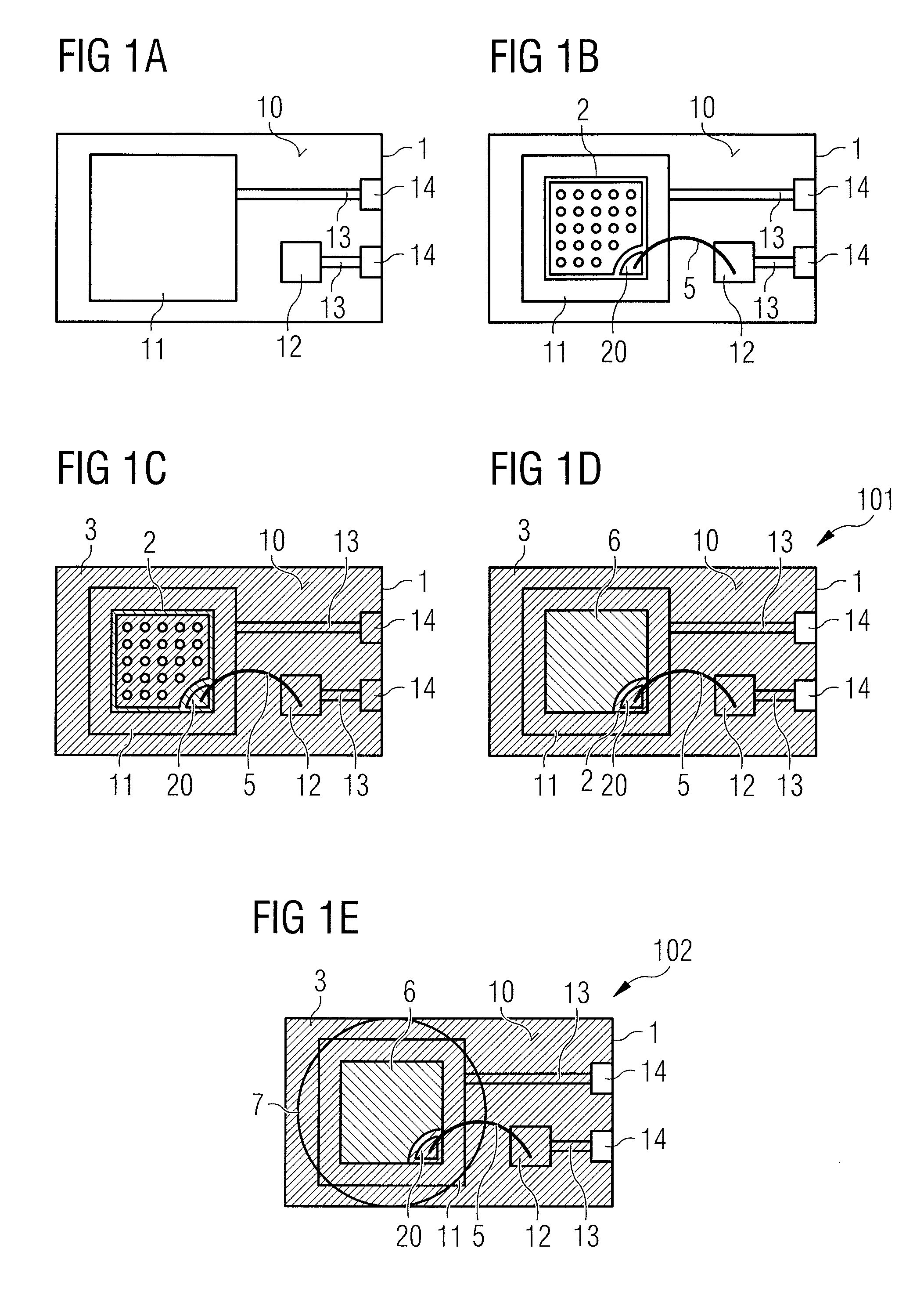
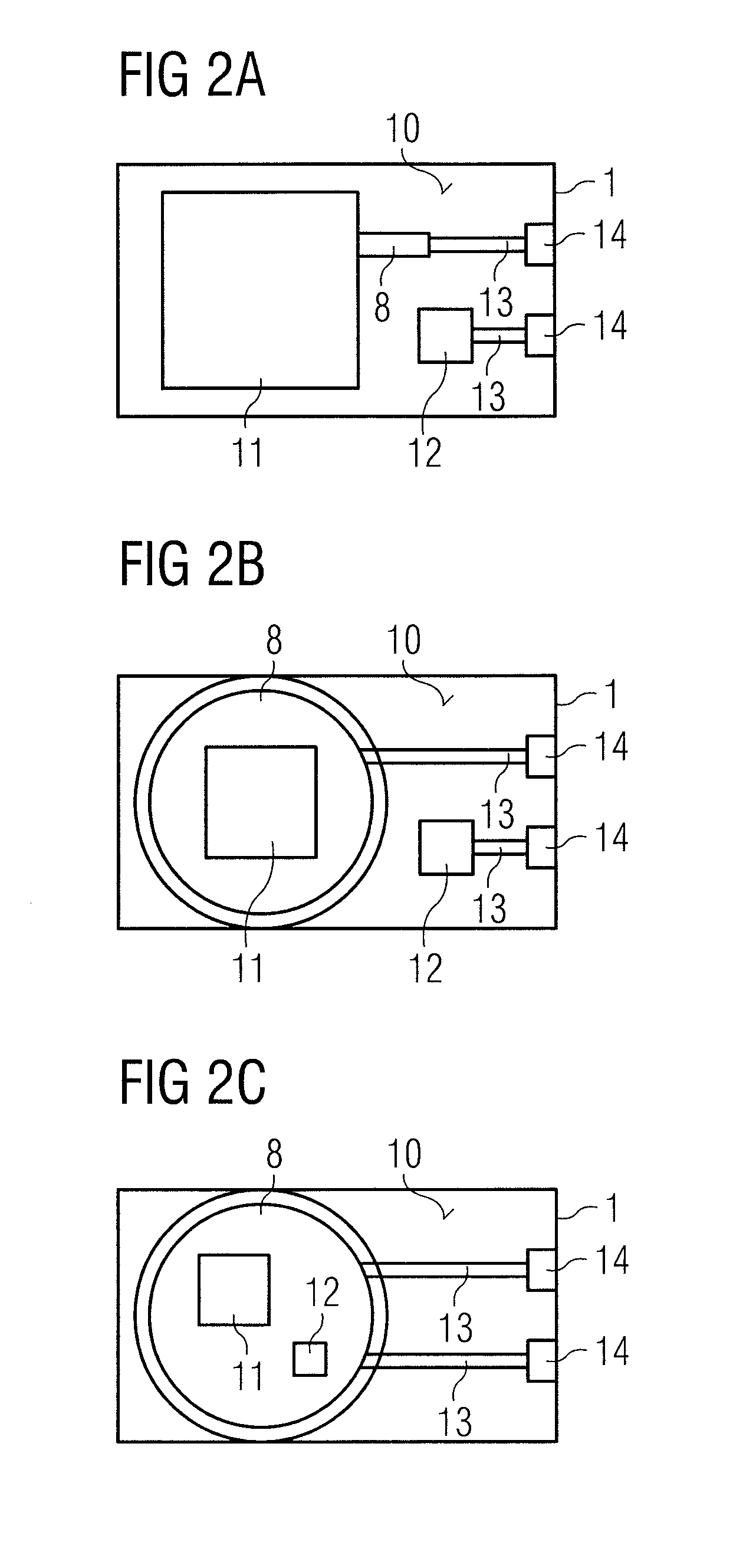
[0049]A method for producing a semiconductor component 101 in accordance with one exemplary embodiment is shown in conjunction with FIGS. 1A to 1D.

[0050]A first method stop in accordance with FIG. 1A involves providing a carrier 1, which has contact regions 11, 12 and also electrical connection regions 14 on a mounting area 10. The contact regions 11, 12 and pad regions 14 are connected to one another by means of conductor tracks 13 on the carrier 1. In particular, in the exemplary embodiment shown, the carrier 1 is embodied as a ceramic carrier, on which the contact regions 11, 12, the connection regions 14 and the conductor tracks 13 are embodied as a coating. The connection regions 14 are embodied as n- and p-type contacts.

[0051]In a further method step in accordance with FIG. 1B, a semiconductor chip 2 is provided and is mounted and electrically connected on the mounting area 10 of the carrier 1.

[0052]The semiconductor chip 2 is mounted and thus simultaneously electrically conne...


PUM


Abstract

A method for producing a light-emitting semiconductor component is specified. A light-emitting semiconductor chip is arranged on a mounting area of a carrier. The semiconductor chip is electrically connected to electrical contact regions on the mounting area. An encapsulation layer is applied to the semiconductor chip by means of atomic layer deposition. All surfaces of the semiconductor chip which are free after mounting and electrical connection are covered with an encapsulation layer. Furthermore, a light-emitting semiconductor component is specified.

Description

[0001]This patent application is a national phase filing under section 371 of PCT / EP2012 / 056536, filed Apr. 11, 2012, which claims the priority of German patent application 10 2011 016 935.0, filed Apr. 13, 2011, each of which is incorporated herein by reference in its entirety.TECHNICAL FIELD[0002]A method for producing a light-emitting semiconductor component and a light-emitting semiconductor component are specified.BACKGROUND[0003]It is known to incorporate light-emitting diode chips in housings or on carriers in order to produce so-called LED packages (LED: light-emitting diode). In such packages, however, the light-emitting diode chips are not completely protected against harmful substances such as, for instance, moisture or in an environment comprising corrosive or otherwise harmful substances such as, for instance, H2S, SO2 and chlorine. This is owing to the fact, inter alia, that potting materials composed of silicone or some other resin are usually used, which have a cert...

Claims


Application Information

Patent Timeline
Patent Type & Authority Applications(United States)
IPC IPC(8): H01L33/52H01L33/60
CPCH01L33/52H01L33/60H01L33/44H01L33/62H01L2933/0025H01L2224/32225H01L2224/48091H01L2924/00014
Inventor ENGL, KARLBAISL, RICHARDSCHLENKER, TILMANHOEPPEL, LUTZTAEGER, SEBASTIANGAERTNER, CHRISTIAN
Owner OSRAM OPTO SEMICONDUCTORS GMBH
Why Eureka
Try Eureka