Batch process for three-dimensional integration

a three-dimensional integration and chip technology, applied in the direction of electrical equipment, semiconductor devices, semiconductor/solid-state device details, etc., can solve the problems of increasing the difficulty of existing inter-chip connections to provide suitable communication characteristics, low power, and difficulty in maintaining the performance of inter-chip interconnections between conventional individually packaged chips that are connected to printed circuit boards. , to achieve the effect of destroying one or more dielectric layers

Active Publication Date: 2013-12-05
ORACLE INT CORP
View PDF6 Cites 22 Cited by
  • Summary
  • Abstract
  • Description
  • Claims
  • Application Information

AI Technical Summary

Benefits of technology

[0013]In some embodiments, the chip package includes one or more dielectric layers disposed on the first surface and/or the second surface. The one or more dielectric layers may exclude chipping damage associated with a singul

Problems solved by technology

As integrated-circuit (IC) technology continues to scale to smaller critical dimensions, it is increasingly difficult for existing inter-chip connections to provide suitable communication characteristics, such as: high bandwidth, low power, reliability and low cost.
For example, as the operating frequencies continue to increase, it is difficult to maintain the performance of inte

Method used


Image

  • Batch process for three-dimensional integration
  • Batch process for three-dimensional integration
  • Batch process for three-dimensional integration

Examples


Embodiment Construction

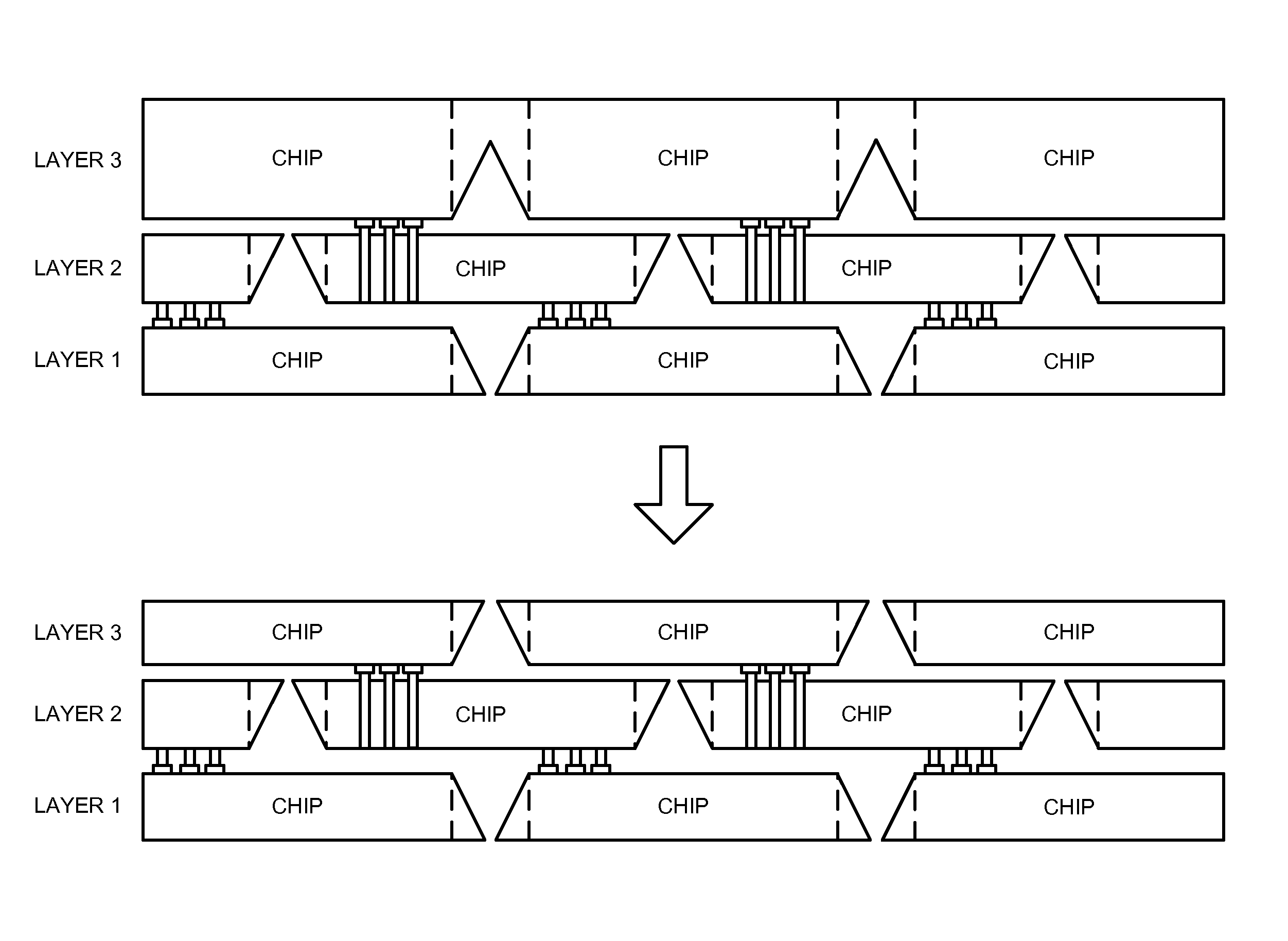
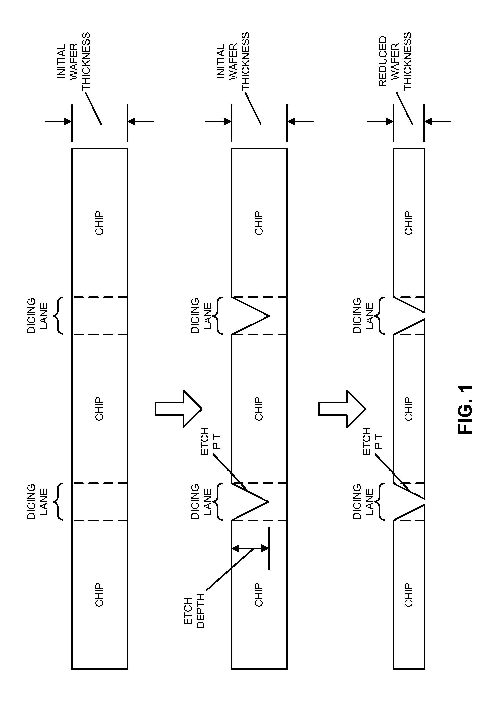
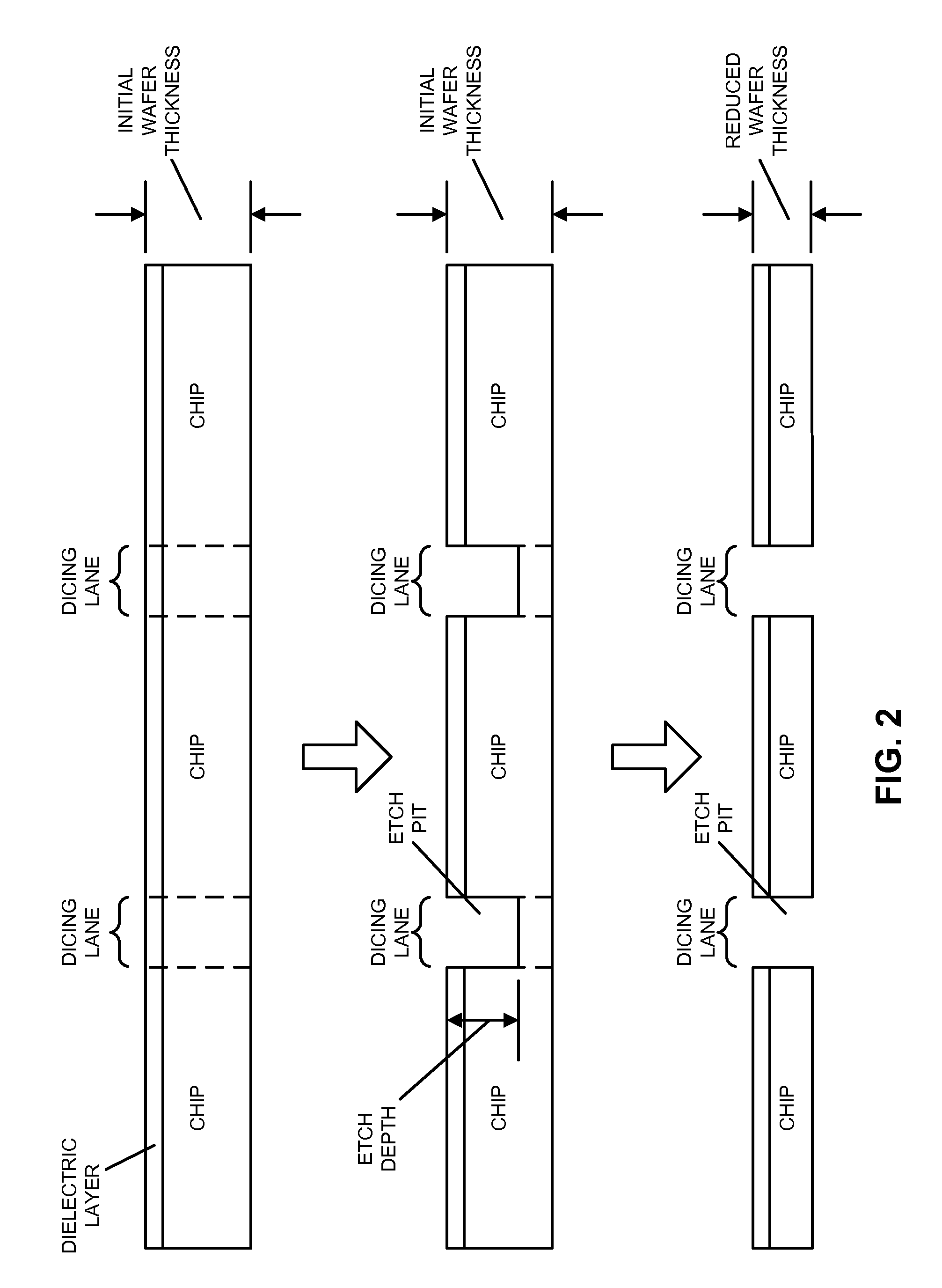
[0030]Embodiments of a chip package and a technique for singulating chips from a wafer are described. This chip package includes a first chip having a first surface and first sides having a first side-wall angle, and a second chip having a second surface and second sides having a second side-wall angle, which faces and is mechanically coupled to the first chip. The chip package is fabricated using a batch process, and the chips in the chip package are singulated from their respective wafers after the chip package is assembled. This is accomplished by etching the first and second side-wall angles and thinning the wafer thicknesses prior to assembling the chip package. For example, the first and / or the second side walls can be fabricated using wet etching or dry etching. Therefore, the first and / or the second side-wall angles may be other than vertical or approximately vertical.

[0031]By facilitating batch processing of the chips in the chip package (as opposed to serially integrating ...


PUM


Abstract

A chip package is described which includes a first chip having a first surface and first sides having a first side-wall angle, and a second chip having a second surface and second sides having a second side-wall angle, which faces and is mechanically coupled to the first chip. The chip package is fabricated using a batch process, and the chips in the chip package were singulated from their respective wafers after the chip package is assembled. This is accomplished by etching the first and second side-wall angles and thinning the wafer thicknesses prior to assembling the chip package. For example, the first and/or the second side walls can be fabricated using wet etching or dry etching. Therefore, the first and/or the second side-wall angles may be other than vertical or approximately vertical.

Description

GOVERNMENT LICENSE RIGHTS[0001]This invention was made with Government support under Agreement No. HR0011-08-9-0001 awarded by DARPA. The Government has certain rights in the invention.BACKGROUND[0002]1. Field[0003]The present disclosure generally relates to the design of a chip package. More specifically, the present disclosure relates to the design of a chip package that facilitates batch-processed, three-dimensional integration.[0004]2. Related Art[0005]As integrated-circuit (IC) technology continues to scale to smaller critical dimensions, it is increasingly difficult for existing inter-chip connections to provide suitable communication characteristics, such as: high bandwidth, low power, reliability and low cost. For example, as the operating frequencies continue to increase, it is difficult to maintain the performance of interconnects between conventional individually packaged chips that are connected to a printed circuit board. As a consequence, engineers are researching alte...

Claims


Application Information

Patent Timeline
IPC IPC(8): H01L23/488H01L21/78
CPCH01L25/0652H01L2924/37001H01L2225/06534H01L24/13H01L24/14H01L24/16H01L24/26H01L24/32H01L24/73H01L24/81H01L24/94H01L25/0657H01L25/50H01L2224/13009H01L2224/131H01L2224/13116H01L2224/13147H01L2224/14181H01L2224/16145H01L2224/26145H01L2224/26175H01L2224/32145H01L2224/72H01L2224/73204H01L2224/81005H01L2224/81203H01L2224/81815H01L2224/83191H01L2224/92125H01L2224/94H01L2225/06513H01L2225/06541H01L2225/06562H01L2225/06531H01L2924/12042H01L24/72H01L2224/81H01L2224/11H01L2924/014H01L2924/00012H01L2224/90H01L2924/00
Inventor THACKER, HIREN D.KRISHNAMOORTHY, ASHOK V.CUNNINGHAM, JOHN E.
Owner ORACLE INT CORP
Why Eureka
Try Eureka