Optical printed circuit board and method for manufacturing the same

a printed circuit board and optical waveguide technology, applied in the direction of optical elements, conductive pattern formation, instruments, etc., can solve the problems of difficult light alignment, difficult light alignment, and limited transmission of mass storage date by electric pcb, so as to reduce the thickness of optical pcb laminated with optical waveguides, easy to align, and increase the aperture area of optical waveguides exposed through the top surface of optical pcb

Inactive Publication Date: 2013-12-05
LG INNOTEK CO LTD
View PDF6 Cites 6 Cited by
  • Summary
  • Abstract
  • Description
  • Claims
  • Application Information

AI Technical Summary

Benefits of technology

[0034]According to the embodiment, since the optical wave guide is configured to have an obtuse curvature, the optical wave guide may not be broken by high tension applied to the optical wave guide, so that the thickness of the optical PCB laminated with the optical wave guide can be reduced.
[0035]In addition, according to the embodiment, the aperture area of the optical waveguide exposed through the top surface of the optical PCB can be increased, so that the optical devices can be readily aligned.
[0036]Further, according to the embodiment, an additional module is provided to hold the optical wave guide at the obtuse angle, so that the stability and the reliability of the optical PCB can be improved.

Problems solved by technology

Since the electric PCB uses conductive metals, such as copper, as electric interconnections for transmitting signals, the electric PCB represents limitations in transmission of mass storage date.
If the optical wave guide 101 has a small sectional area, light alignment is difficult.
As described above, if the optical wave guide is vertically laminated, the section of the optical wave guide exposed through the top surface of the optical PCB has the area equal to the vertical sectional area of the optical wave guide, and the light alignment is difficult if the optical wave guide has a small sectional area.
In addition, since the optical path changing part is manufactured by bending the optical wave guide at the right angle to change the optical path at the right angle, light loss may be generated due to the bending structure of the optical wave guide and the optical wave guide may be broken caused by high tension as the bending work is carried out.

Method used


Image

  • Optical printed circuit board and method for manufacturing the same
  • Optical printed circuit board and method for manufacturing the same
  • Optical printed circuit board and method for manufacturing the same

Examples


first embodiment

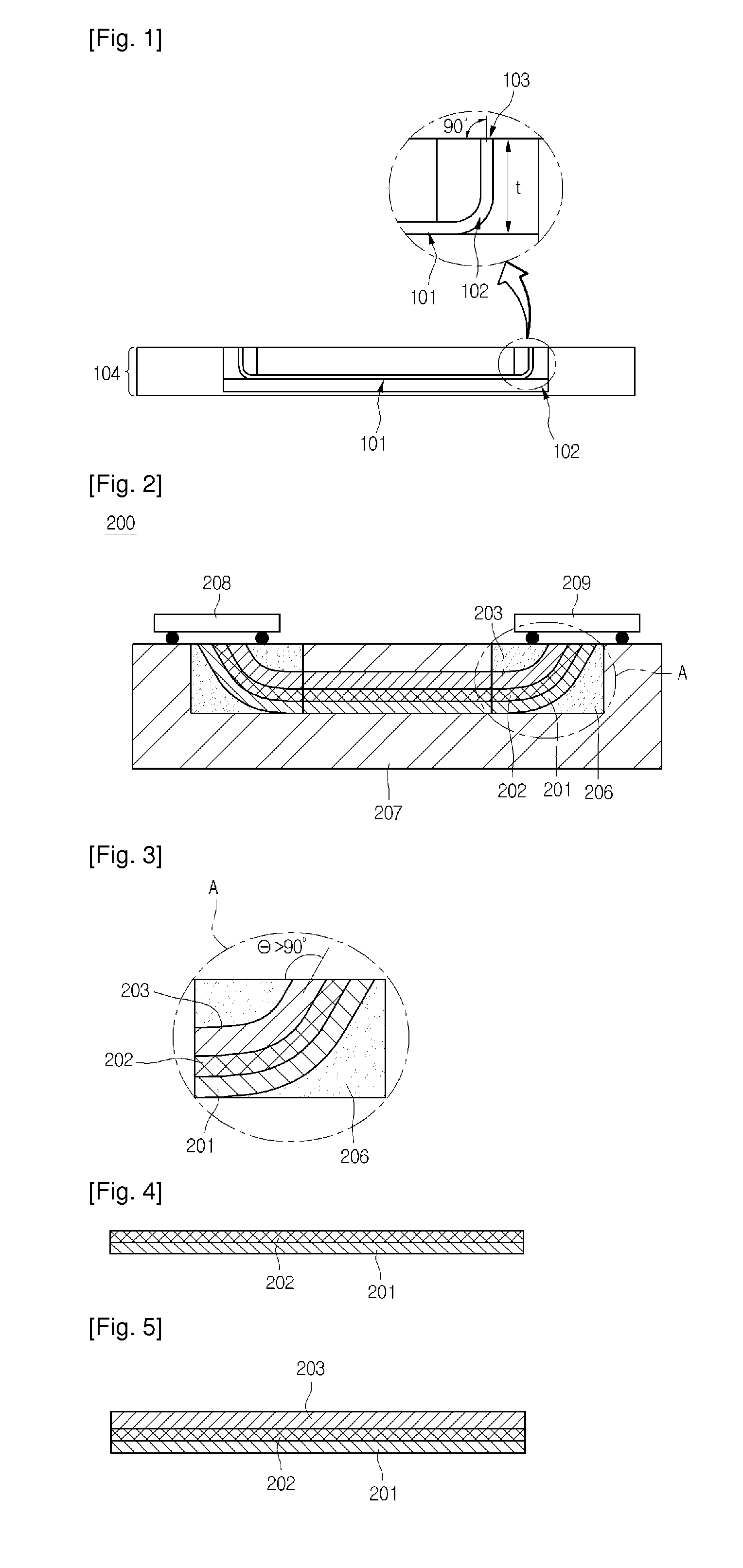
[0046]Hereinafter, an optical PCB will be described with reference to FIGS. 2 to 10.

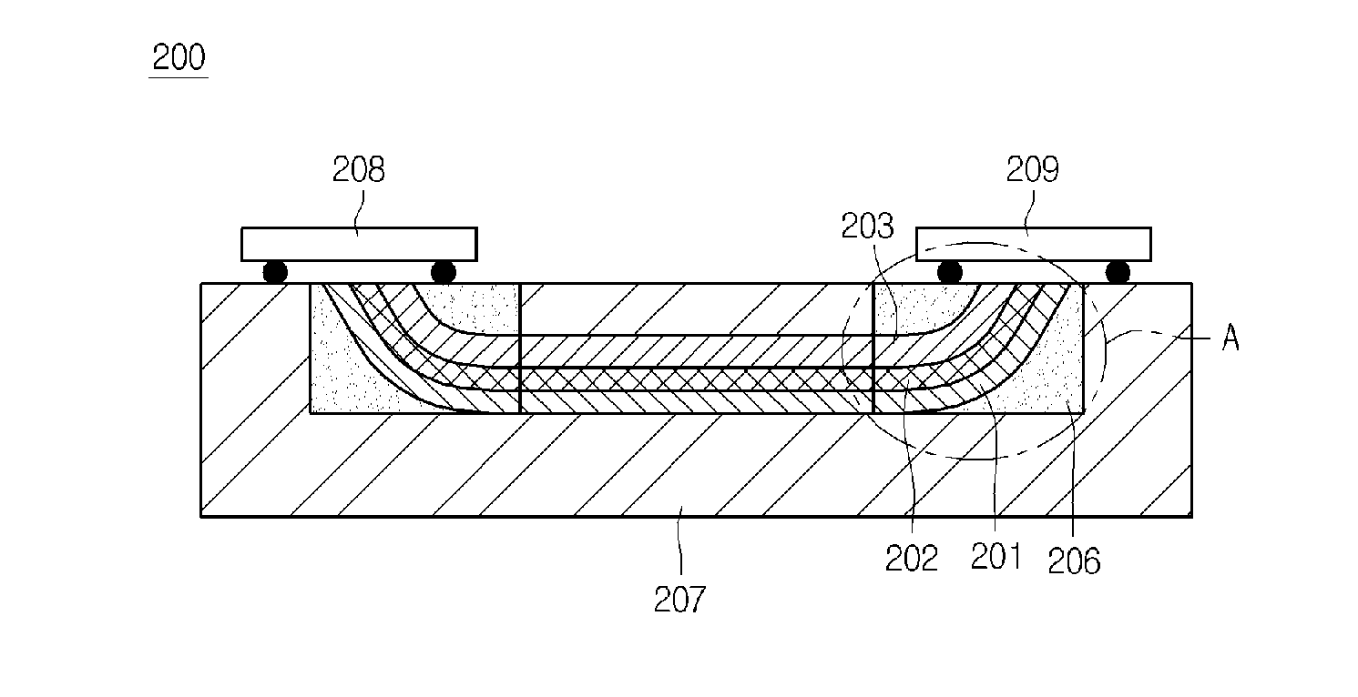
[0047]FIG. 2 is a sectional view showing an optical PCB according to the first embodiment.

[0048]Referring to FIG. 2, the optical PCB 200 according to the first embodiment includes a base substrate 207, an optical wave guide 210 laminated in the base substrate 207 to form an optical path, an optical path changing part 206 formed on at least one end of the optical wave guide 210 to allow the optical path defined by the optical wave guide 210 to have a predetermined curvature of an obtuse angle, a light transmitter 208 laminated on the base substrate 207 to transmit the light, and a light receiver 209 to receive the light transmitted from the light transmitter 208.

[0049]The base substrate 207 may include a circuit pattern (not shown) to perform electric signal transmission with respect to an insulating layer. The circuit pattern may include an electric conductive metal, such as Au, Ag, Ni or Cu. Accord...

second embodiment

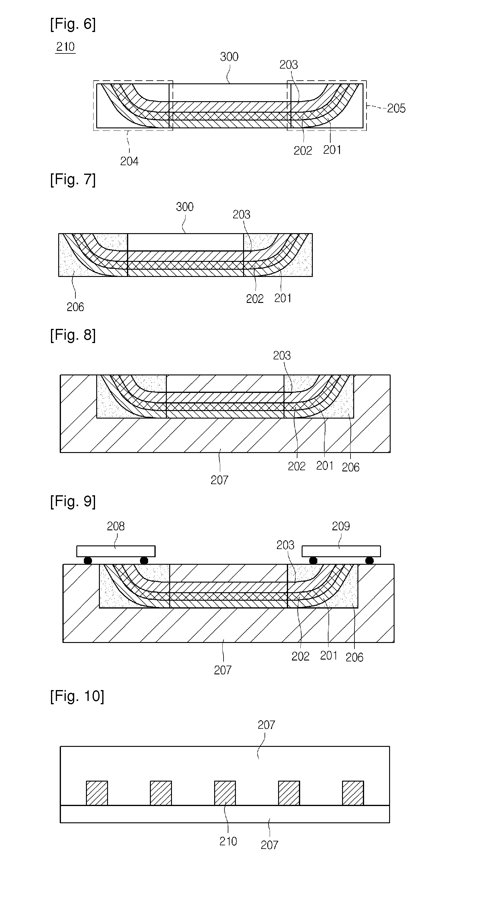
[0112]FIG. 11 is a sectional view showing an optical PCB according to the

[0113]Referring to FIG. 11, the optical PCB 400 according to the second embodiment includes a base substrate 407, an optical wave guide 410 laminated in the base substrate 407 to form an optical path, an optical path changing part 406 formed on at least one end of the optical wave guide 410 to allow the optical path defined by the optical wave guide 410 to have a predetermined curvature of an obtuse angle, a light transmitter 408 laminated on the base substrate 407 to transmit the light, and a light receiver 409 to receive the light transmitted from the light transmitter 408.

[0114]The base substrate 407 may include a circuit pattern (not shown) to perform electric signal transmission with respect to an insulating layer. The circuit pattern may include an electric conductive metal, such as Au, Ag, Ni or Cu. According to the present embodiment, Cu is used for the circuit pattern.

[0115]Preferably, the base substra...


PUM

PropertyMeasurementUnit
bending angleaaaaaaaaaa
transmission pathaaaaaaaaaa
optical pathaaaaaaaaaa

Abstract

An optical printed circuit board according to the embodiment includes an insulating layer; an optical wave guide buried in the insulating layer to transmit an optical signal; and an optical path converting part provided on at least one end of the optical wave guide to convert a transmission path of the optical signal defined by the optical wave guide such that the transmission path has a predetermined curvature.

Description

TECHNICAL FIELD[0001]The embodiment relates to an optical printed circuit board and a method for manufacturing the same.BACKGROUND ART[0002]In general, a printed circuit board (PCB) is manufactured by using a copper clad laminate in which a conductive layer is laminated on an insulating member. The PCB can be manufactured by forming circuit patterns on the copper clad laminate, which is called an electric PCB. Since the electric PCB uses conductive metals, such as copper, as electric interconnections for transmitting signals, the electric PCB represents limitations in transmission of mass storage date.[0003]In order to solve the above problem, recently, an optical PCB including an optical wave guide formed on an insulating member has been developed. In order to form the optical wave guide serving as an optical path in the optical PCB, optical fiber including polymer or glass fiber is employed.[0004]FIG. 1 shows a sectional view of an optical PCB according to the related art as well ...

Claims


Application Information

Patent Timeline
Patent Type & Authority Applications(United States)
IPC IPC(8): G02B6/125
CPCG02B6/125G02B6/43H05K1/0274H05K2201/10121Y10T29/49155
Inventor LEE, HYOUN JEONG
Owner LG INNOTEK CO LTD
Why Eureka
Try Eureka