Circuit layout method for printed circuit board, eletronic device and computer readable recording media

a circuit layout and printed circuit board technology, applied in the field of circuit layout methods and electronic devices, can solve the problems of instability in the product system, affecting the quality and stability of the signal trace, and the impedance value of the specific signal trace to vary and become incorrect, so as to increase the yield rate of finished products and improve the quality and efficiency of circuit layou

Inactive Publication Date: 2013-12-05
WISTRON CORP
View PDF9 Cites 10 Cited by
  • Summary
  • Abstract
  • Description
  • Claims
  • Application Information

AI Technical Summary

Benefits of technology

[0007]Henceforth, an exemplary embodiment of the present disclosure provides a circuit layout method for printed circuit board. The provided method can automatically establish corresponding keep-out region in circuit layout according to the requirement of signal quality during circuit design process, thereby increase the quality and the efficiency of the circuit layout, further increases the yield rate of finished product.

Problems solved by technology

Hence, whenever a signal trace on PCB is referencing the wrong reference layer, would cause the impedance value of the specific signal trace to vary and become incorrect.
The transmission quality and stability of the signal trace will be affected which in turns causes instability in the product system, or causes the product not been able to function at all.
Consequently, the finished PCB becomes scrap and increases the overall product development time and cost.
This not only reduces the design efficiency but also easy for operator to have omissions.
Additionally, the corresponding inspection also requires the operator to conduct manually hence very easily to have misjudgments or omissions, causing the finished product malfunctions thereby increase the product cost.

Method used


Image

  • Circuit layout method for printed circuit board, eletronic device and computer readable recording media
  • Circuit layout method for printed circuit board, eletronic device and computer readable recording media
  • Circuit layout method for printed circuit board, eletronic device and computer readable recording media

Examples


first exemplary embodiment

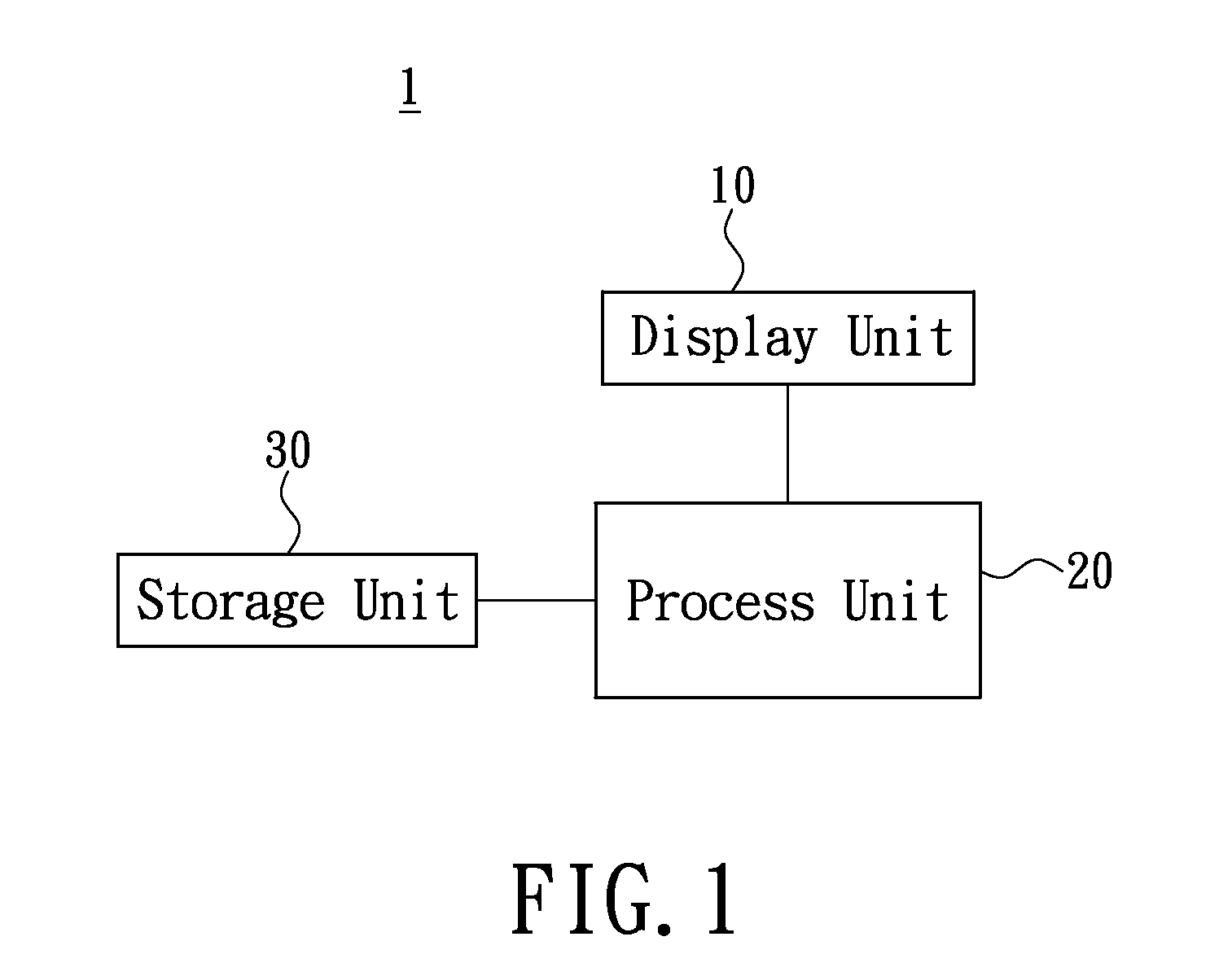
[0033]Please refer to FIG. 1, which is a block diagram illustrates an electronic device provided in accordance to the first exemplary embodiment of the present disclosure. The electronic device 1 includes a display unit 10, a processing unit 20, and a storage unit 30. The display unit 10 and the storage unit 30 are coupled to the processing unit 20, respectively. The electronic device 1 in the instant embodiment may be implemented by a computer device, such as a desktop, a notebook or a tablet, however, the present disclosure is not limited thereto.

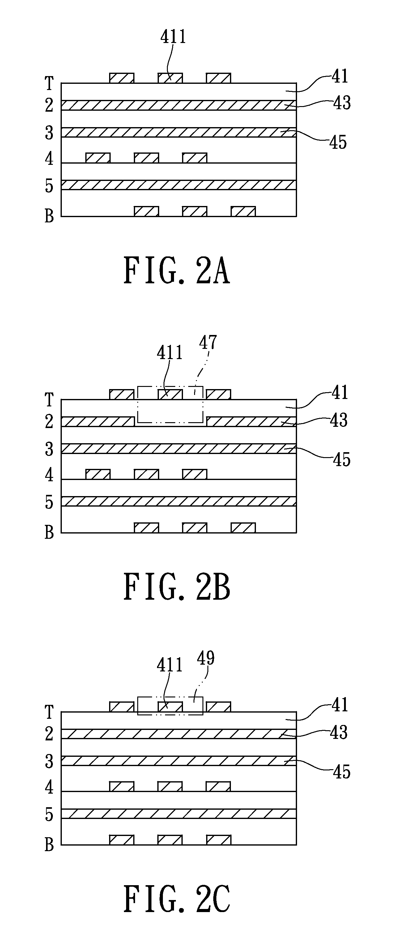
[0034]The display unit 10 is used for displaying a parameter configuration interface (not shown in FIG. 1), for a designer to input parameter data corresponding to a circuit layout of a printed circuit board. The parameter data includes stack-up parameters and layout parameters. Specifically, the stack-up parameters include the controlled radio frequency layers and the corresponding keep-out layers. The layout parameters include the layou...

second exemplary embodiment

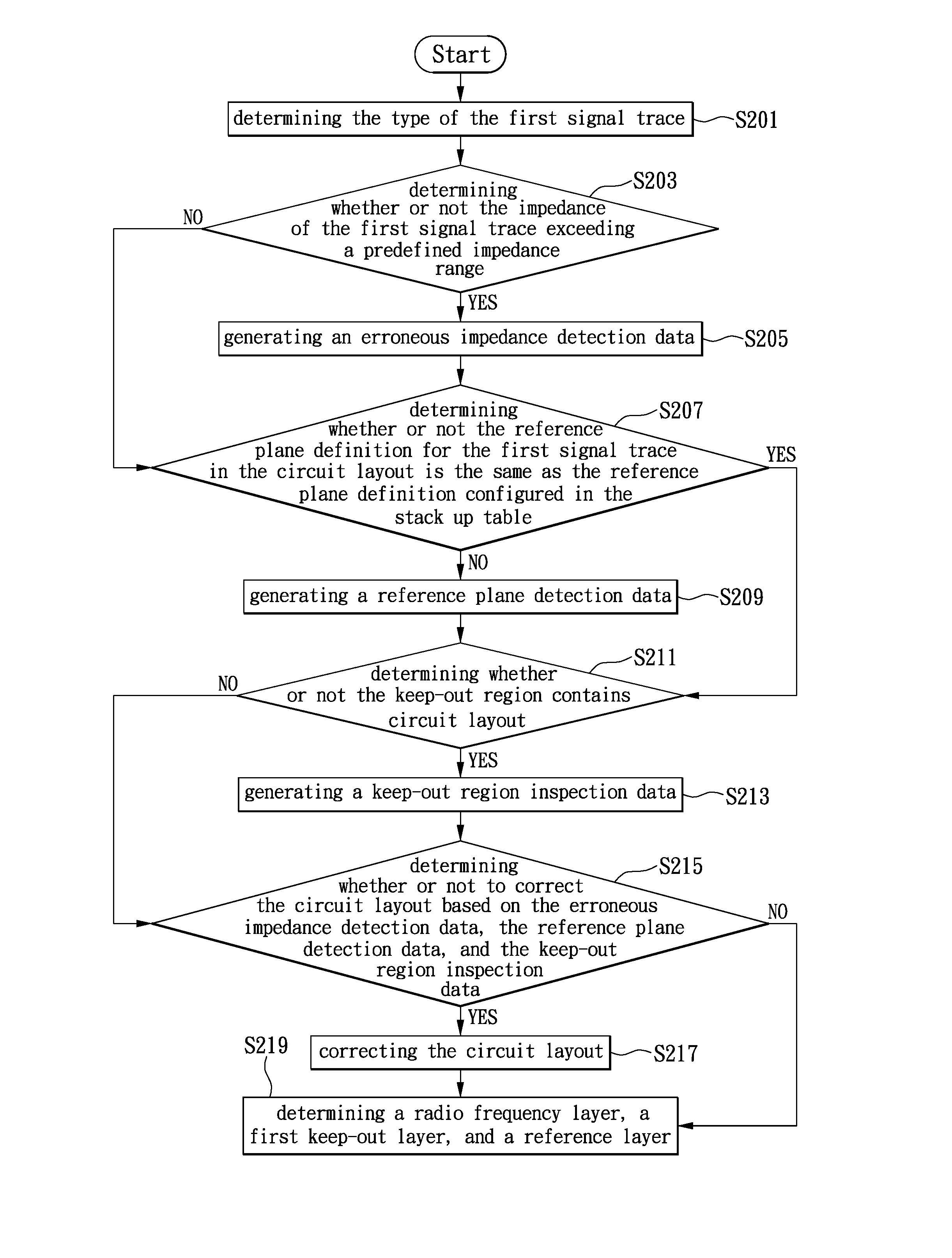
[0060]According to the above-mentioned exemplary embodiment, the present disclosure may generalize a circuit layout method for printed circuit board which can be adapted to the electronic device of the above-mentioned exemplary embodiment. Please refer to FIG. 5-1 and FIG. 5-2, in conjunction to FIG. 1. FIG. 5-1 and FIG. 5-2 are flowchart diagrams respectively illustrating a circuit layout method for a printed circuit board provided in accordance to the second exemplary embodiment of the present disclosure.

[0061]First, in the step S101, the processing unit 20 receives the stack-up parameters and a plurality of layout parameters inputted by the designer through a parameters configuration interface displayed on the display unit 10. The stack-up parameters includes the controlled radio frequency layers according to the circuit layout requirements and the corresponding keep-out layers. The layout parameters include the definition of the layout object being disposed on the signal trace b...


PUM


Abstract

The present disclosure illustrates a circuit layout method for printed circuit board which is adapted for an electronic device. The circuit layout method includes the following steps. A parameters configuration interface is provided for receiving corresponding stack-up parameters and a plurality of layout parameters. A radio frequency layer, a first keep out layer, and a reference layer are determined based on the stack-up parameters. The first keep-out layer is placed between the radio frequency layer having a first signal trace disposed thereon and the reference layer. A first keep-out region on the first keep-out layer is formed in corresponding to the first signal trace. Circuit layouts disposed inside the first keep-out region are removed. Consequently, the corresponding keep-out region may be automatically generated in accordance to the signal requirements of the signal trace while designing the circuit layout thereby increase circuit layout quality and efficiency thereof.

Description

BACKGROUND[0001]1. Technical Field[0002]The present disclosure relates to a circuit layout method and an electronic device thereof, in particular, to a circuit layout method for printed circuit board, an electronic device thereof and a computer readable recording medium.[0003]2. Description of Related Art[0004]When designing the circuit layout on a printed circuit board (PCB), certain traces (e.g., single-end trace or differential trace) may require impedance control according to the product design requirement, such as configuring corresponding trace width, spacing, length, thickness, and so on) to obtain the desired signal transmission quality.[0005]In circuit layout design, regardless whether the reference layer of which the signal trace corresponds to is placed in adjacent to the signal trace or not all have decisive impact on the impedance of the signal trace being controlled. Hence, whenever a signal trace on PCB is referencing the wrong reference layer, would cause the impedan...

Claims


Application Information

Patent Timeline
Patent Type & Authority Applications(United States)
IPC IPC(8): G06F17/50
CPCG06F17/5081G06F2119/10G06F30/39G06F30/398
Inventor YU, WEI-FANTENG, I-PING
Owner WISTRON CORP
Why Eureka
Try Eureka