Interposer substrate, electronic device package, and electronic component

Inactive Publication Date: 2013-12-19
THE FUJIKURA CABLE WORKS LTD
View PDF10 Cites 2 Cited by
  • Summary
  • Abstract
  • Description
  • Claims
  • Application Information

AI Technical Summary

Benefits of technology

The invention achieves smaller and more dense three-dimensional packaging that can prevent an increase in thickness of the substrate even when the number of through-hole interconnections increases. It also provides more flexibility in designing the wiring structure and reduces the size of electronic devices and components.

Problems solved by technology

When highly-densified three-dimensional packaging is carried out by use of a plurality of through-hole interconnections in the above-described interposer substrate, there are technical problems.
However, in order to avoid a malfunction, which is caused by mutual interference, while maintaining electrical insulation between the adjacent through-hole interconnections, it is not possible to decrease the distance L between the separate through-hole interconnections without limitation.
Such increase in the substrate thickness is undesirable in terms of downsizing and thinning of a high-density package.

Method used


Image

  • Interposer substrate, electronic device package, and electronic component
  • Interposer substrate, electronic device package, and electronic component
  • Interposer substrate, electronic device package, and electronic component

Examples


first embodiment

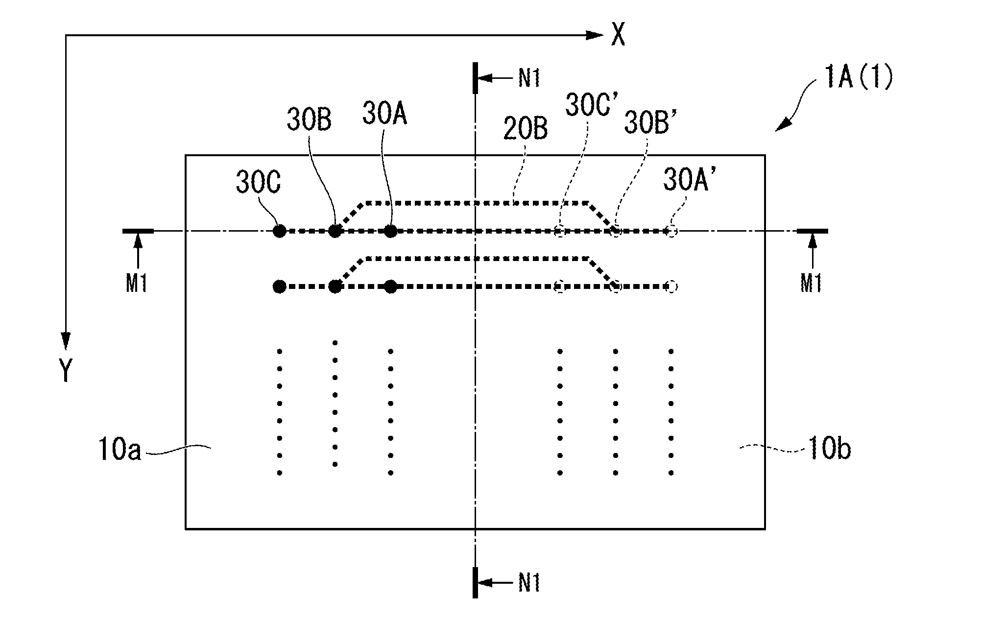
[0070]FIGS. 1 to 4 schematically show a configuration example of an interposer substrate of the first embodiment of the invention.

[0071]Here, FIG. 1 is a plan view illustrating a state where a plurality of terminal groups are arranged on a top face in the interposer substrate of the first embodiment of the invention.

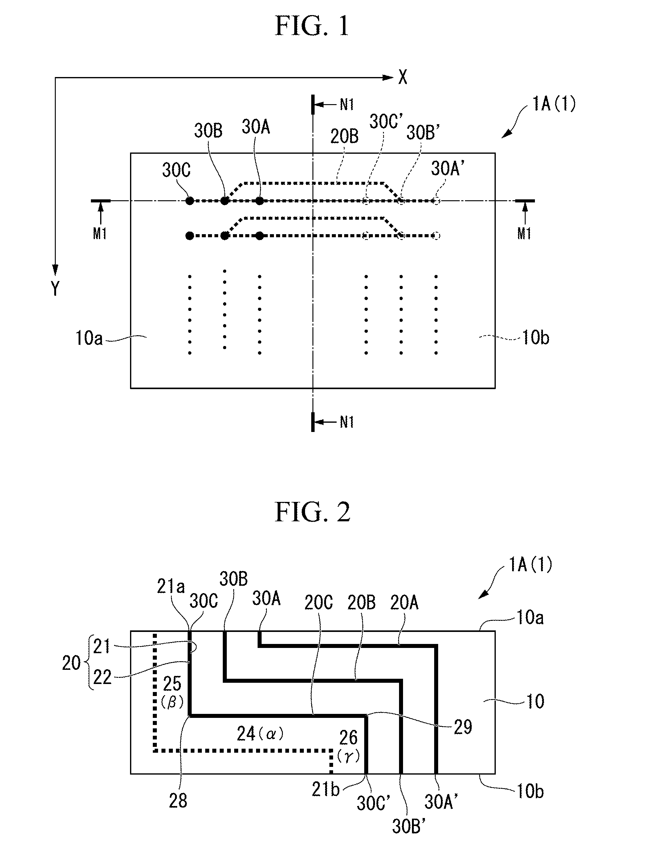
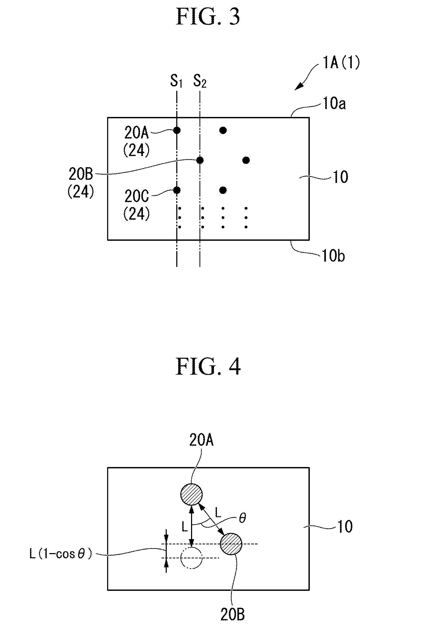
[0072]Additionally, FIG. 2 is a cross-sectional view taken along the line M1-M1 shown in FIG. 1, and FIGS. 3 and 4 are cross-sectional views taken along the line N1-N1 shown in FIG. 1.

[0073]An interposer substrate 1A (1) is provided with a plurality of through-hole interconnections 20A, 20B, and 20C (20) which connect main surfaces (the first main surface 10a and the second main surface 10b) constituting a single the substrate 10.

[0074]As a material used to form the substrate 10, an insulator such as glass, plastic, ceramics, or the like, a semiconductor such as silicon (Si) or the like is adopted.

[0075]In a case where a semiconductor substrate is used as a material used...

second embodiment

[0117]Next, a second embodiment of the invention will be described.

[0118]Additionally, in the interposer substrate 1A (1) of a second embodiment as shown in FIG. 5, pads 2 and 3 may be provided on the main surfaces 10a and 10b of the substrate 10, respectively, so as to electrically connect the second portion 25 and the third portion 26 constituting the through-hole interconnection 20.

[0119]When the devices are mounted onto both faces of the interposer substrate 1A (1), even in cases where a downsized device in which the electrodes are densely arranged with any layout is used, since the electrodes of the devices and the pads are electrically connected to each other without front wirings, a downsized device can be connected to the interposer substrate.

[0120]Furthermore, in the interposer substrate 1A (1), the lengths of the through-hole interconnections 20A, 20B, and 20C are preferably substantially the same as each other.

[0121]Because of this, the electrical resistances of the throu...

third embodiment

[0123]Next, a third embodiment of the invention will be described.

[0124]Additionally, in the interposer substrate 1A (1), the substrate 10 may include a cooling unit cooling the substrate 10.

[0125]As such cooling unit cooling the substrate 10, for example, a flow passage 40 allowing a cooling fluid to flow therein is adopted as shown in FIG. 5.

[0126]By means of this structure, even in cases where a device having a large amount of heat generation is mounted onto the interposer substrate, an increase in temperature can be reduced by applying a cooling medium to the flow passage 40.

[0127]The flow passage 40 includes outlet-inlet ports 40a and 40b which are provided at both ends of the flow passage 40 and which discharge and supply the cooling fluid.

[0128]For example, a plurality of flow passages 40 may be provided.

[0129]Furthermore, the flow passage 40 may be provided so as to wind its way so that a single flow passage 40 can cool over the entirety of the substrate 10.

[0130]Additionall...


PUM


Abstract

An interposer substrate of the invention includes: a single substrate having a first main surface and a second main surface; and a plurality of through-hole interconnections having first portions formed so as to extend in parallel with each other and connecting the first main surface to the second main surface, wherein the through-hole interconnections adjacent to each other are provided so that ideal axes are parallel to each other with a distance therebetween, and the ideal axes extend perpendicular to at least one of the first main surface and the second main surface and penetrate through centers of the first portions.

Description

CROSS REFERENCE TO RELATED APPLICATIONS[0001]This application is a continuation application based on a PCT Patent Application No. PCT / JP2012 / 062157, filed May 11, 2012, whose priority is claimed on Japanese Patent Application No. 2011-107580 filed on May, 12, 2011, the content of which is hereby incorporated by reference.BACKGROUND OF THE INVENTION[0002]1. Field of the Invention[0003]The present invention relates to an interposer substrate, an electronic device package using the same, and an electronic component which are provided with through-hole interconnections realizing a SiP (system in package) in which a high-density package such as an electronic device, an optical device, a MEMS device, or the like or such devices are systemized in a single package.[0004]2. Description of the Related Art[0005]In recent years, with the higher performance of electronic devices such as portable telephones or the like, higher speed and higher performance are required for electronic devices or th...

Claims


Application Information

Patent Timeline
IPC IPC(8): H05K1/11H05K7/00
CPCH05K1/115H05K7/005H01L23/49827H01L25/0657H01L2225/06517H01L2225/06572H01L2224/16225H01L2924/15172H01L2924/15182H01L2924/157H01L2924/15787H01L2924/15788H01L2924/1579H01L2924/1461H01L2924/00
Inventor YAMAMOTO, SATOSHIWAKIOKA, HIROYUKI
Owner THE FUJIKURA CABLE WORKS LTD
Why Eureka
Try Eureka