Thin film silicon solar cell in tandem junction configuration on textured glass

a technology of tandem junction and solar cell, applied in the field of thin film silicon solar cell, can solve the problems of light scattering properties of surface textured substrate, limit the ultimate cell efficiency,

Inactive Publication Date: 2013-12-26
CORNING INC +1
View PDF4 Cites 5 Cited by
  • Summary
  • Abstract
  • Description
  • Claims
  • Application Information

AI Technical Summary

Problems solved by technology

A general disadvantage of this design is a trade off between the “optical thickness” of the absorber layer (which should be large in order to enhance absorption) and the distance between the electrodes—“electrical thickness”, which should be small to reduce the influence of the Staebler-Wronski effect on cell efficiency in a long term.
This however limits the ultimate cell efficiency even when deposited on a good quality light scattering TCO optimized for maximal light trapping in the subsequent Si layer.
Light scattering properties of surface textured substrates have become an important issue in the process of optimization of thin-film solar cell performance.

Method used


Image

  • Thin film silicon solar cell in tandem junction configuration on textured glass
  • Thin film silicon solar cell in tandem junction configuration on textured glass
  • Thin film silicon solar cell in tandem junction configuration on textured glass

Examples


examples

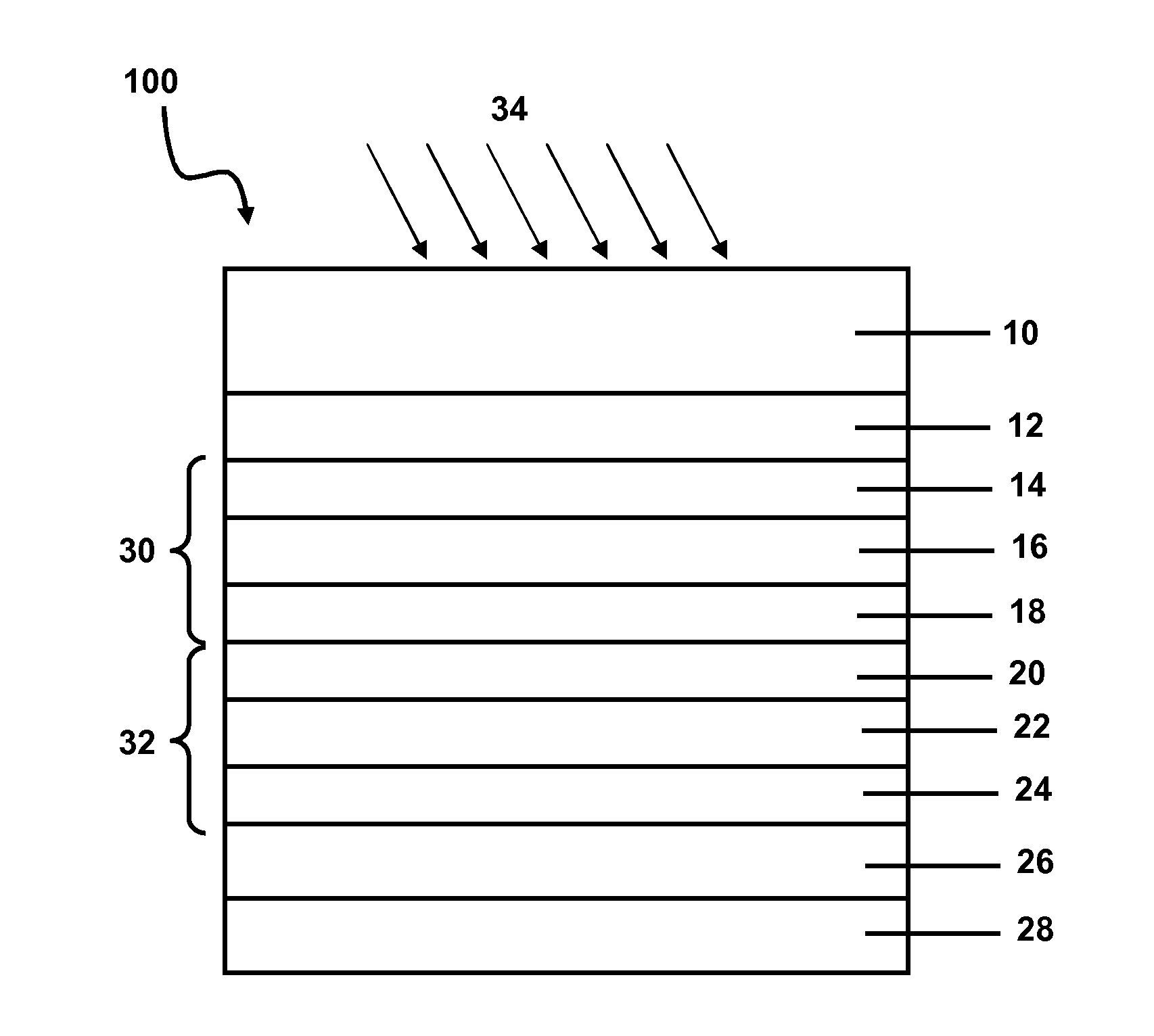
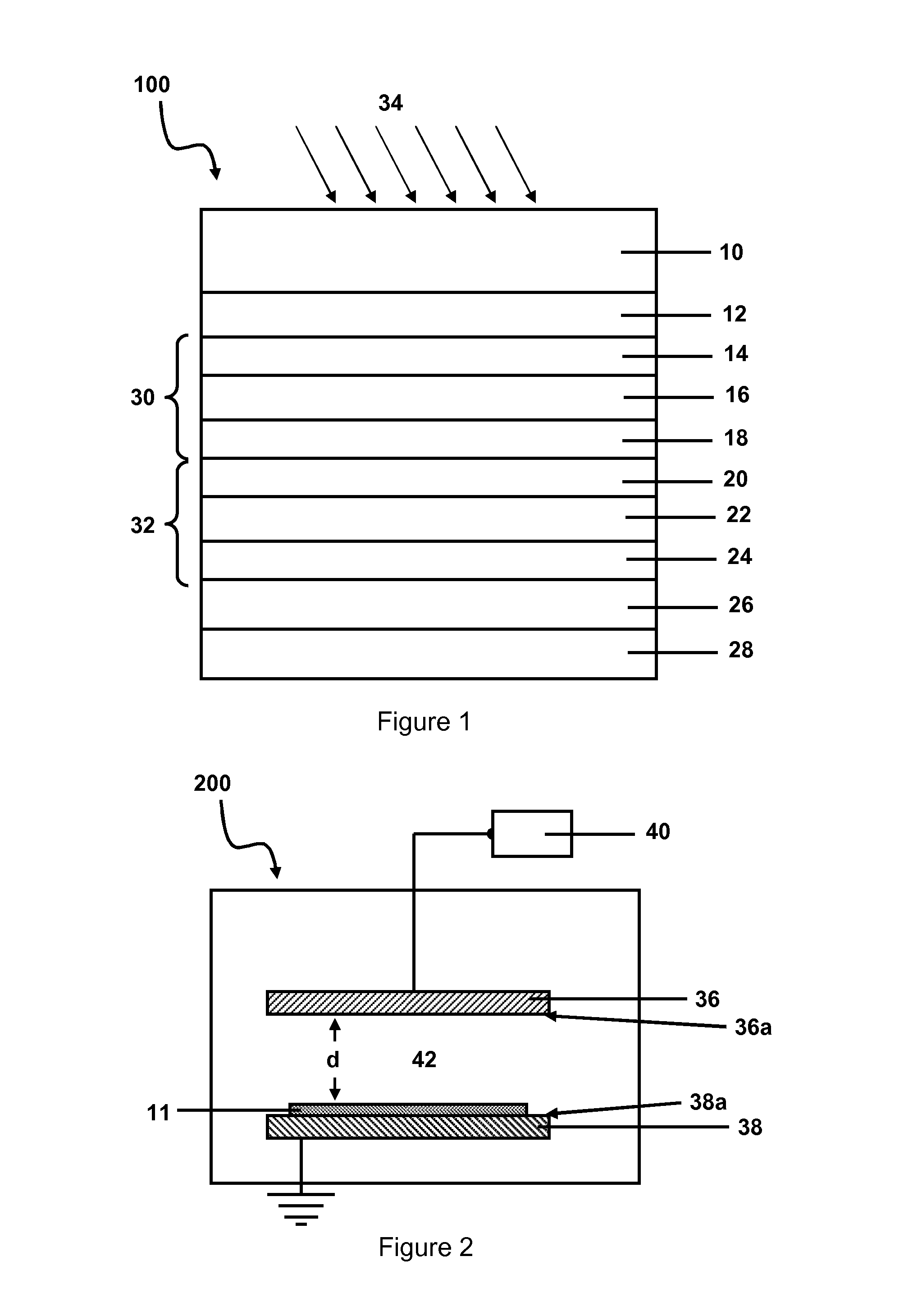
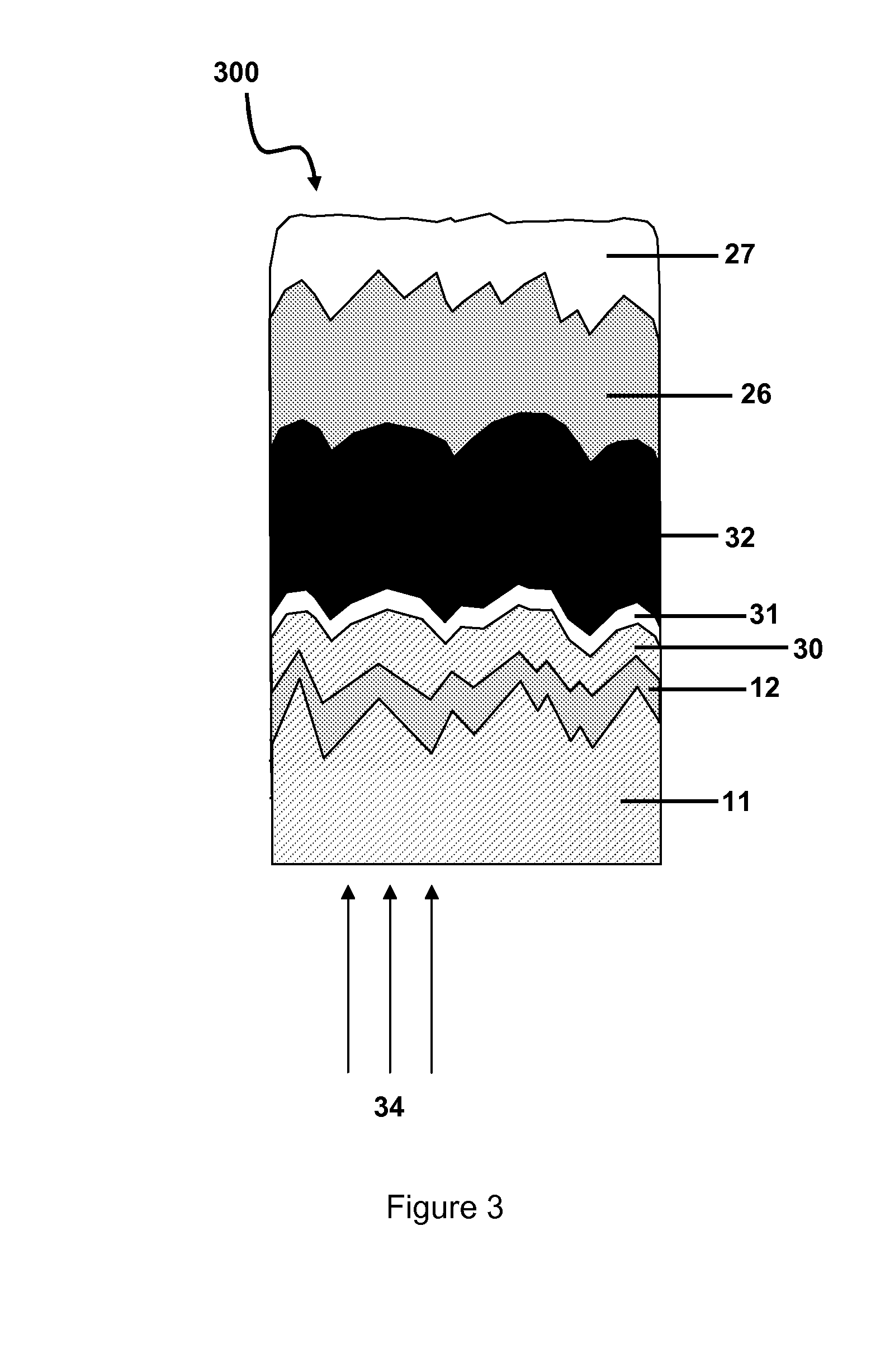
[0079]A thin-film silicon tandem junction, according to one embodiment, was manufactured by deposition by PECVD equipment known as an Oerlikon Solar KAI PECVD reactor. To improve deposition rates for solar-grade amorphous and microcrystalline silicon these reactors run with radio frequency (RF) power at a excitation frequency of 40.68 MHz. The results described below have been obtained in KAI-M (520×410 mm2) reactors. One focus had been laid on the further development of the front and back ZnO contact (=electrodes 12, 26 shown in FIG. 1) for optimized Micromorph cell efficiencies. These rough as-grown ZnO layers are deposited by low pressure chemical vapor deposition (LPCVD) from diethylzinc as precursor material. Such a LPCVD process and deposition system are described in U.S. Pat. No. 7,390,731 (incorporated herein by reference). The TCO roughness enhances the light-trapping within the active layers of the tandem cell. In one embodiment, the TCO comprises B-doped ZnO.

[0080]The PEC...


PUM


Abstract

Solar cells or solar modules of the so-called tandem type, i.e. stacked arrangements of photovoltaic absorber devices on a substrate with a textured surface are described. The thin film solar cell has a substrate comprising a textured surface, and a front electrode layer comprising a transparent conductive oxide adjacent to the textured surface, wherein the electrode layer has a thickness less than the roughness of the textured surface.

Description

[0001]This application claims the benefit of priority under 35 U.S.C. §119 of U.S. Provisional Application No. 61 / 379,844 filled on Sep. 3, 2010 the contents of which is relied upon and incorporated herein by reference in its entirety.BACKGROUND[0002]1. Field[0003]Embodiments relate generally to solar cells or solar modules of the so-called multi-junction type, for example, silicon tandem, i.e. stacked arrangements of photovoltaic absorber devices on a substrate with a textured surface.[0004]2. Technical Background[0005]FIG. 1 is an illustration of a tandem-junction silicon thin film solar cell as known in the art. Such a thin film solar cell 100 usually includes a first or front electrode 12, one or more semiconductor thin film p-i-n junctions (top cell 30 having layers 14, 16, and 18, and bottom cell 32, having layers 20, 22, and), and a second or back electrode 26, which are successively stacked on a substrate 10. Each p-i-n junction 30, 32 or thin-film photoelectric conversion u...

Claims


Application Information

Patent Timeline
Patent Type & Authority Applications(United States)
IPC IPC(8): H01L31/0236H01L31/076
CPCH01L31/0236H01L31/076H01L31/022466H01L31/02366H01L31/03921H01L31/022483Y02E10/548Y02E10/50
Inventor BAILAT, JULIENKOCH, III, KARL WILLIAMKOHNKE, GLENN ERICMARJANOVIC, SASHAMEIER, JOHANNES
Owner CORNING INC
Why Eureka
Try Eureka