Thermal process for creation of an in-situ junction layer in CIGS

a technology of in-situ junction layer and solar cell, which is applied in the field of photovoltaics, can solve the problems of difficult commercial scale of these processes, inability of pv cells to effectively replace traditional energy sources in the market, and efficient thin-film manufacturing process, and achieve the effect of reducing the temperature of the substra

Inactive Publication Date: 2006-05-18
DAYSTAR TECHNOLOGIES
View PDF0 Cites 91 Cited by
  • Summary
  • Abstract
  • Description
  • Claims
  • Application Information

AI Technical Summary

Benefits of technology

[0009] In a preferred embodiment, the n-type layer is formed as a continuation of a treatment whereby the CIGS is being exposed to an activity of In, Ga and Se at elevated temperatures less than 460° C. In such an embodiment, the activity of In, Ga and Se does not substantially change, but the temperature of the substrate is decreased either intentionally, or as a consequence of natural cooling from higher temperatures, to the point where the activity of In, Ga and Se no longer reacts with the CIGS absorber layer. Instead, these elements deposit and form its own compound in the form of an (In,Ga)ySe n-type layer that serves both as a junction partner and as a buffer between the CIGS and the intrinsic ZnO layer that follows. The intrinsic transparent oxide layer supports a transparent conducting oxide layer and a top metal grid.

Problems solved by technology

Relatively efficient photovoltaic (“PV”) cells can be manufactured in the laboratory; however, it has proven difficult to commercially scale these processes with the consistent repeatability and efficiency critical for commercial viability.
The lack of an efficient thin-film manufacturing process has contributed to the failure of PV cells to effectively replace traditional energy sources in the market.
Without an efficient thin-film manufacturing process, PV cells cannot effectively replace current energy sources.
However, the multiple layers comprising a PV device offer challenges to a mass production system.
Presently, there is no proven technology for continuously producing CIGS devices.
Additionally, the typical PV cell manufacturing technique involves batch processing that necessitates touch labor, high capital costs, and low manufacturing output.
CIGS systems, in particular, pose unique challenges to manufacturers.
However, this process is problematic.
Moreover, this process creates hazardous waste, the disposal of which is a challenge to potential manufacture.
While some alternatives to the CBD CdS process have been proposed, none are viable options in the context of large scale continuous manufacturing.
However, inserting these alternative buffer layers often involve more chemical steps, as well as post deposition anneals or light soaking to become fully active.
Adding these post-deposition steps decreases the efficiency of the manufacturing process, and subjects the product to potential mishandling and contamination.

Method used


Image

  • Thermal process for creation of an in-situ junction layer in CIGS
  • Thermal process for creation of an in-situ junction layer in CIGS

Examples


Embodiment Construction

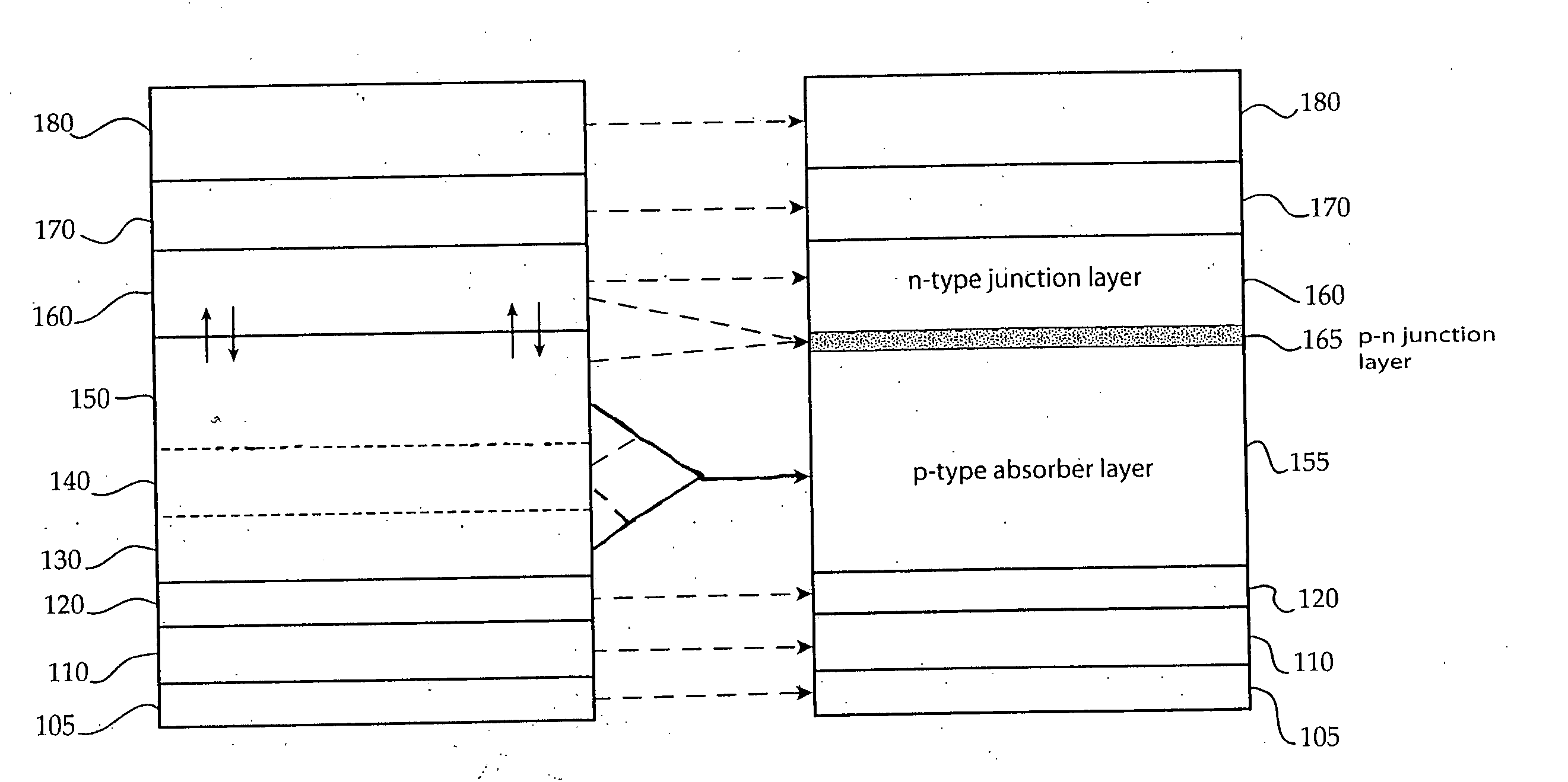
[0011] Chalcopyrite ternary thin films of copper-indium-diselenide (CuInSe2) and copper-indium-gallium-diselenide (CuIn1-x Gax Se2), both of which are generically referred to as Cu(In, Ga)Se2, or CIGS, have become the subject of considerable interest and study for semiconductor devices in recent years. Sulfur can also be, and sometimes is, substituted for selenium, so the compound is sometimes also referred to even more generically as Cu(In,Ga)(Se, S)2 so as to encompass all of these possible combinations. These devices are also referred to as I-III-VI2 devices according to their constituent elemental groups. These devices are of particular interest for photovoltaic device or solar cell absorber applications. For photovoltaic applications, the p-type CIGS layer is combined with an n-type CdS layer to form a p-n heterojunction CIGS / CdS device.

[0012] The direct energy gap of CIGS results in a large optical absorption coefficient, which in turn permits the use of thin layers on the or...


PUM

PropertyMeasurementUnit
temperatureaaaaaaaaaa
thicknessaaaaaaaaaa
temperatureaaaaaaaaaa

Abstract

The present invention relates generally to the field of photovoltaics and more specifically to manufacturing thin-film solar cells using a thermal process. Specifically, a method is disclosed to manufacture a CIGS solar cell by an in-situ junction formation process.

Description

CROSS-REFERENCE TO RELATED APPLICATIONS [0001] This application claims priority from U.S. Provisional Patent Application Ser. No. 60 / 626,843, filed Nov. 10, 2004.FIELD OF THE INVENTION [0002] The invention disclosed herein relates generally to the field of photovoltaics and more specifically to creating thin-film solar cells using an in-situ junction process. BACKGROUND OF THE INVENTION [0003] Relatively efficient photovoltaic (“PV”) cells can be manufactured in the laboratory; however, it has proven difficult to commercially scale these processes with the consistent repeatability and efficiency critical for commercial viability. The lack of an efficient thin-film manufacturing process has contributed to the failure of PV cells to effectively replace traditional energy sources in the market. Translating laboratory batch processing methods into effective industrial processes that are both cheaper and better controlled would help advance PV technology to mainstream markets. [0004] Wit...

Claims


Application Information

Patent Timeline
Patent Type & Authority Applications(United States)
IPC IPC(8): H01L31/00H01L21/00
CPCC23C14/568H01L31/0322H01L31/072H01L31/0749H01L31/1876Y02E10/541Y02P70/50
Inventor TUTTLE, JOHN R.
Owner DAYSTAR TECHNOLOGIES
Why Eureka
Try Eureka