Method for Forming Light Absorption Layer of Cis Type Thin-Film Solar Cell

a technology of cis type and solar cell, which is applied in the direction of solid-state diffusion coating, sustainable manufacturing/processing, and final product manufacturing, etc., can solve the problems of poor quality or performance of the solar cell as a whole, unfavorable direct use of this technique for the formation of the light absorption layer of the cis type thin-film solar cell, and uneven solar cell performance. achieve the effect of improving the state of b, improving the quality, and improving the flow of rea

Inactive Publication Date: 2008-05-15
SHOWA SHELL SEKIYU KK
View PDF5 Cites 92 Cited by
  • Summary
  • Abstract
  • Description
  • Claims
  • Application Information

AI Technical Summary

Benefits of technology

[0023]The invention employs an atmosphere-homogenizing device for making the temperature in the apparatus even and for improving the state of being in contact with reactant gases and chalcogen elements (selenium and sulfur) and the manner of work disposition which enables a reactant gas to circulate smoothly. By such simple device and manner, the temperature in the apparatus is made even and the state of being in contact with the reactant gas and a chalcogen element (selenium and sulfur) is improved. Thus, the light absorption layers of CIS type thin-film solar cells which are simultaneously formed can be made to have even and improved quality (component proportion) and performances. In addition, the solar cell performances of CIS type thin-film solar cells and the yield of the products can be improved.

Problems solved by technology

As a result, a light absorption layer in which the proportions of components are uneven is formed, resulting in uneven solar cell performances.
Furthermore, the performances of a solar cell are adversely influenced by any defective part in the work treated for film formation (in the case where given quality or performance is not satisfied) and the presence of such a defective part disadvantageously results in the fabrication of a solar cell which as a whole has poor quality or performances.
Because of this, it is difficult to directly use this technique for the formation of the light absorption layer of a CIS type thin-film solar cell.
Moreover, the furnace described in patent document 1, which is a furnace having therein baffles serving as the circulating passages, has a complicated constitution and is expensive.
Use of the technique hence has had a problem that production cost increases.

Method used


Image

  • Method for Forming Light Absorption Layer of Cis Type Thin-Film Solar Cell
  • Method for Forming Light Absorption Layer of Cis Type Thin-Film Solar Cell
  • Method for Forming Light Absorption Layer of Cis Type Thin-Film Solar Cell

Examples


Embodiment Construction

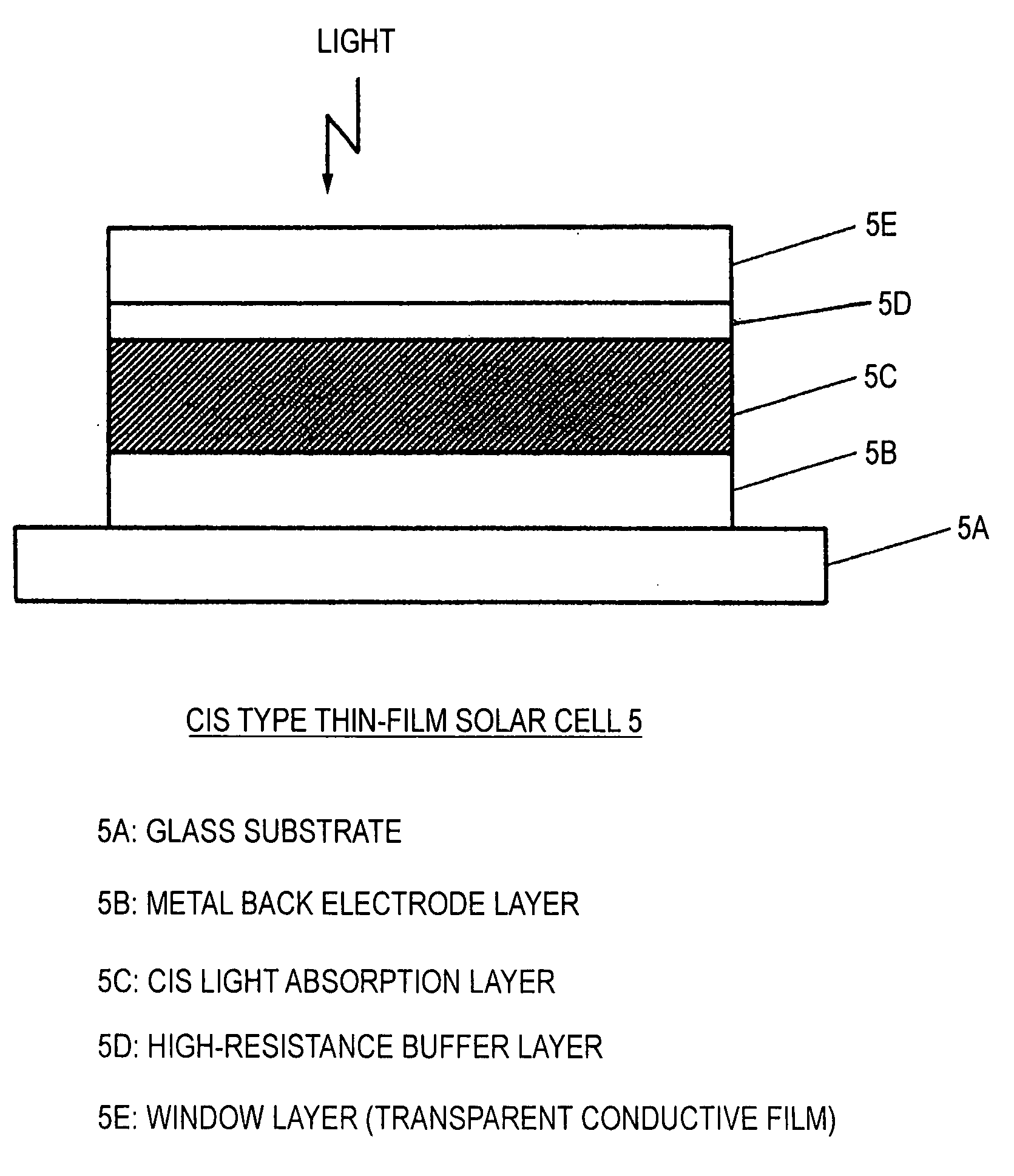
[0024]The invention provides a method of film formation for use in the step of film formation by selenization, sulfurization / selenization, sulfurization, or selenization / sulfurization among steps for forming the CIS light absorption layer in a CIS type thin-film solar cell. As shown in FIG. 7, a CIS type thin-film solar cell 5 is a pn heterojunction device of a substrate structure comprising a glass substrate SA, a metal back electrode layer SB, a p-type CIS light absorption layer 5C, a high-resistance buffer layer 5D, and an n-type window layer (transparent conductive film) 5E which have been superposed in this order. When the CIS light absorption layer 5C is formed, a metallic precursor film of a multilayer structure (hereinafter referred to as work to be treated for film formation) comprising any one of Cu / Ga (work 2A), Cu / In (work 2B), and Cu-Ga / In (work 2C) as shown in FIG. 5 on a metal back electrode layer 5B on a glass substrate is subjected to the step of film formation by s...


PUM

PropertyMeasurementUnit
temperatureaaaaaaaaaa

Abstract

A simple device is used to make the temperature in an apparatus even and improve the state of being in contact with reactant gases, selenium, and sulfur.A fan 3 as a device for atmosphere homogenization is disposed in an apparatus, and the work is disposed in the manner which enables a reactant gas to circulate smoothly. Namely, flat platy works 2 are disposed apart from each other at a certain distance parallel to the direction of the major axis of the apparatus while keeping the plates vertical so that the apparatus has passages within the group of works and has gas passages over and under the works and on both sides thereof. Thus, each work is apt to come into contact with the reactant gases in the apparatus and the temperature in the apparatus is even. The state of being in contact with the reactant gases, selenium, and sulfur is improved.

Description

TECHNICAL FIELD[0001]The present invention relates to a method for forming the light absorption layer of a CIS type thin-film solar cell.BACKGROUND ART[0002]A CIS type thin-film solar cell is a pn heterojunction device having a substrate structure comprising a glass substrate, a metal back electrode layer, a p-type CIS light absorption layer, a high-resistance buffer layer, and an n-type window layer which have been superposed in this order, as shown in FIG. 7. When the CIS light absorption layer is formed, a metallic precursor film of a multilayer structure (hereinafter referred to as work to be treated for film formation) comprising any one of Cu / Ga (work 2A), Cu / In (work 2B), and Cu-Ga / In (work 2C) as shown in FIG. 5 on a metal back electrode layer on a glass substrate is selenized or sulfurized to form the CIS light absorption layer. A method of film formation which has been used for selenizing or sulfurizing the work to be treated for film formation comprises disposing such wor...

Claims


Application Information

Patent Timeline
Patent Type & Authority Applications(United States)
IPC IPC(8): H01L31/00
CPCC23C8/00C23C8/02C23C8/06Y02E10/541C23C12/00C23C14/5866H01L31/0322C23C10/02H01L31/1864Y02P70/50H01L31/18H01L31/0445
Inventor ONODERA, MASARUKURIYAGAWA, SATORUTANAKA, YOSHIAKI
Owner SHOWA SHELL SEKIYU KK
Why Eureka
Try Eureka