Sensor arrangement with electrically controllable arrays

a sensor array and array technology, applied in the field of electrical controllable arrays of sensors, can solve the problems of inability to read out prior described electrode arrays by serial methods usual in computer technology, and the actual sensoric function has to be taken over by additional optical components, so as to avoid interference in polarization and eliminate undesired binding events

Inactive Publication Date: 2007-04-24
FRAUNHOFER GESELLSCHAFT ZUR FOERDERUNG DER ANGEWANDTEN FORSCHUNG EV
View PDF15 Cites 121 Cited by
  • Summary
  • Abstract
  • Description
  • Claims
  • Application Information

AI Technical Summary

Benefits of technology

[0055]Simultaneously using the ultramicroelectrodes for detection, optionally supplemented by further auxiliary electrodes, as elements for effecting electrophoretic transportation processes of the analyte molecules to the positions of affinity-binding partner molecules and also for eliminating undesired binding events, is of particular advantage.
[0056]Interferences in polarization are avoided by an arrangement for electric control which continuously supplies the arrays which are no longer addressed with a polarization voltage. The continuous supply lasts until the subsequent addressing time at which an information of the sensor position is again inquired. Said electric control during non-addressing time intervals is adapted to provide a current supply, preferably by a substantially galvanic or ohmic connection from a corresponding array to a source supplying the potential, particularly far off the sensor position.

Problems solved by technology

A disadvantage of all electric sensor array arrangements having been described so far and comprising electrodes as transducers, is that they are only suited for mono analyte determination, or that the actual sensoric function has to be taken over by additional optical components.
Moreover, prior described electrode arrays could not be read out by serial methods usual in computer technology, i.e. subsequently, without disturbing the electric double layer which is formed by polarization at the electrodes in voltammetric detection methods.

Method used


Image

  • Sensor arrangement with electrically controllable arrays
  • Sensor arrangement with electrically controllable arrays
  • Sensor arrangement with electrically controllable arrays

Examples


embodiments

EXAMPLE 1

Production of an Electric Sensor Array with Direct Output Contact in Silicon Technology

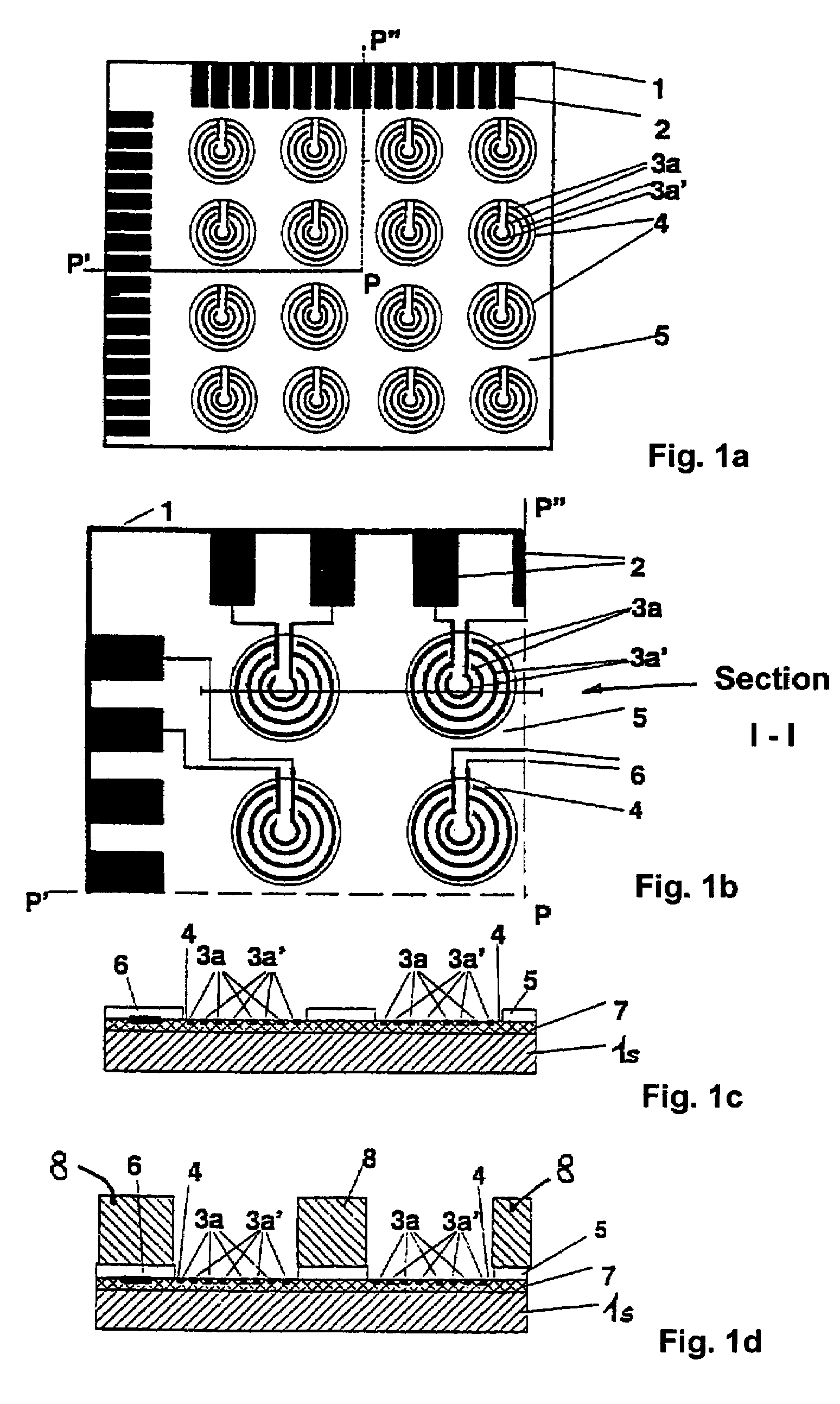
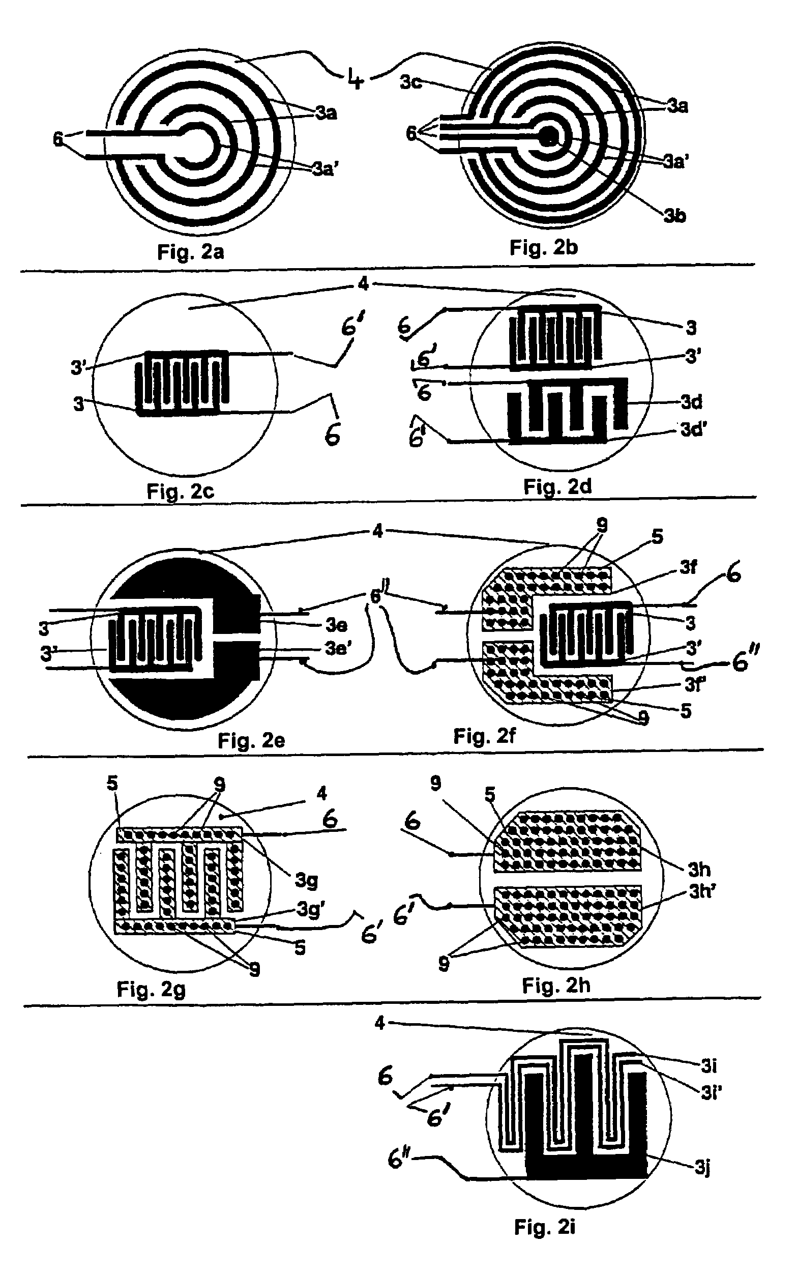
[0158]Microelectrode structures according to FIGS. 1 and 2a are produced by standard silicon technology, compare Reimer et al., Sensors and Actuators, A 46 / 47(1995) 66. A thermal oxide of a thickness of 500 nm is produced on 4″ silicon wafers. On said oxide, a photo resist is photolithographically structured such that the contours of the electrodes are uncovered for the electrode structures. An ultramicroelectrode system of concentric rings according to FIG. 2a comprises annular electrode strips having a width of 1.5 μm and an ring distance of 800 nm. The rings are alternately connected with the contacts according to FIG. 2a via conducting paths 6. 16 sensor positions are arranged on the sensor array in a 4×4 matrix with array positions of a diameter of 300 μm. 2×16 output contacts are arranged on two adjacent sides of a silicon chip having a size of 1×1 cm. The distances of the sensor ar...

example 2

Production of an Electric Sensor Array with a Direct Contacting on Glass

[0160]Interdigital electrode arrays according to FIG. 2e, having 9 sensor positions are structured in a 3×3 matrix on 4″-Pyrex-glass-wafers by a photolithography according to example 1. Unlike example 1, an adhesive chromium layer of a thickness of 20 nm, followed by a platinum layer of a thickness of 150 nm are evaporated onto the glass and finally structured by a lift-off method according to example 1. As an adhesion agent for the subsequent insulating layer, a 3% solution of alkyloxysilane in acetone is brought into contact with the surface. After centrifuging a polyimide layer of a thickness of 10 μm thereupon, the sensor array positions, which have a size of 400 μm and are positioned at a distance of 500 μm with respect to each other, are structured by a standard photolithography such that the contact surfaces and the sensor positions are uncovered. An interdigital electrode system with auxiliary electrodes...

example 3

Production of an Electric Sensor Array System with CMOS Switches

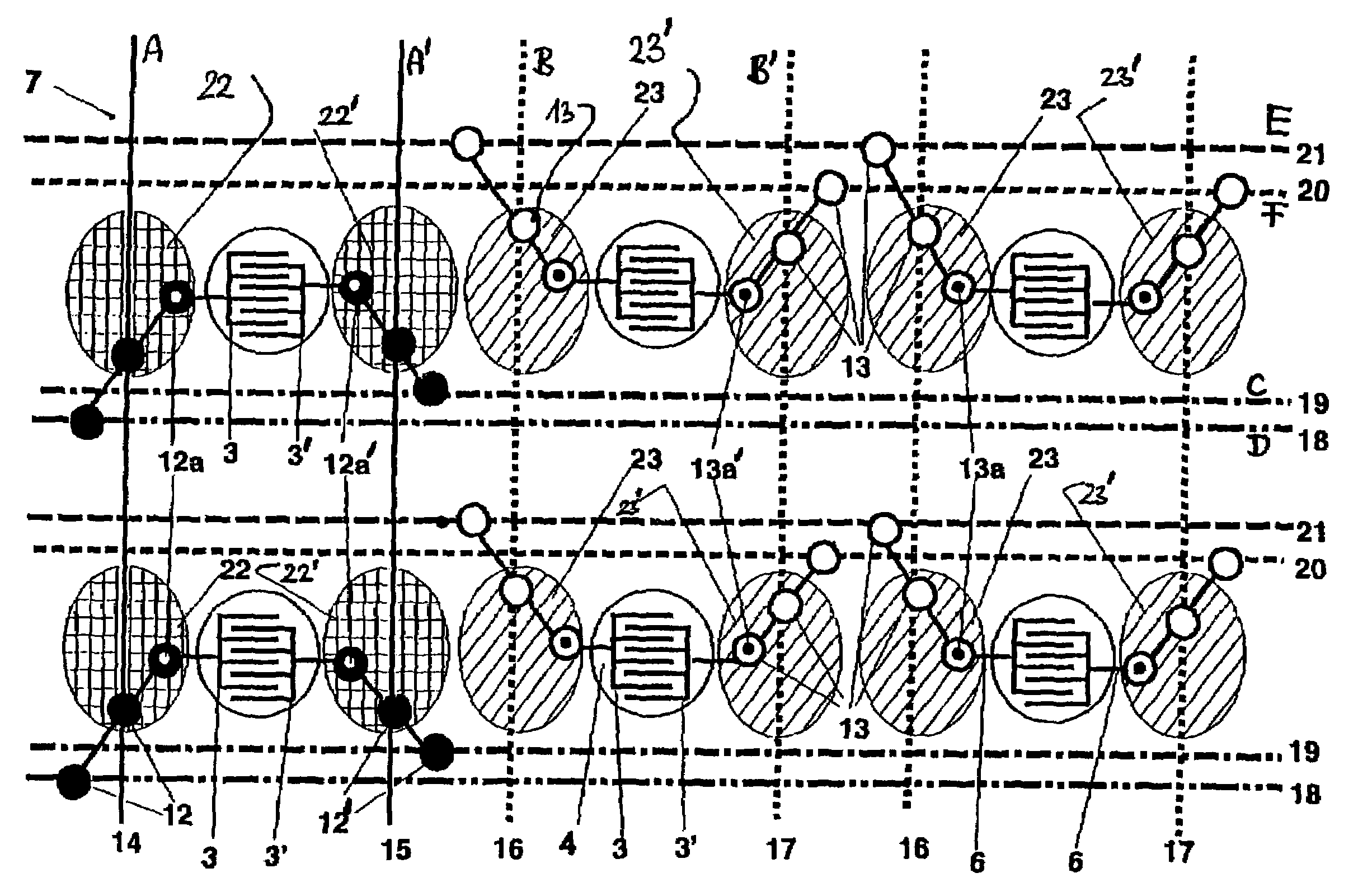
[0161]A switch plane is produced by a CMOS standard method, compare Widmann, Mader, Friedrich, Technologie hochintegrierter Schaltungen, Springer Verlag Berlin 1996, in a process with 1 μm minimum structures. Crossings of conducting paths required according to FIG. 3 are realized by crossovers 32 of polysilicon paths 31a and aluminum paths 27. A higher electric resistance is not of importance due to small sensor currents. In the CMOS method used, switches 12, 12′ and 13, 13′ are advantageously adapted as transmission gates. A transmission gate connects the points 12a, 12a′ with line 18 and 19, and the points 13a, 13a′ with bias line 21 and 20. Addressing lines 14, 15, 16, 17 comprise a pair of conducting paths extending in parallel, at which signals of a complementary polarity are supplied to the gates of the two transistors of a transmission gate. Alternatively, an on-chip inverter may produce two complementary signals...


PUM

PropertyMeasurementUnit
structural widthaaaaaaaaaa
widthaaaaaaaaaa
diameteraaaaaaaaaa

Abstract

An electric sensor array which is provided with several sensor positions that each have at least two microelectrodes. Molecular substances can be detected electrochemically and charged molecules can be transported or handled using the array. Measuring procedures can be effected, especially using two addressing procedures, in which sensor positions can be individually addressed and electrochemically or electrically controlled by pairing or in groups for voltage or impedance measurements. For biomolecular assays, affinity-binding molecules can be immobilized at the sensor positions, between the microelectrodes, or on auxiliary surfaces.

Description

[0001]This application is a 371 of PCT / EP00 / 03404, filed Apr. 14, 2000, which claims priority from DE 19916921.7, filed Apr. 14, 1999, and PCT / EP99 / 04883, filed Jul. 12, 1999.FIELD OF INVENTION[0002]The invention relates to an electric sensor array and methods using multiple ultramicroelectrodes as electrochemical transducers and to be used as a component of measuring arrangements for simultaneously detecting different molecules from mixtures of substances in biochemical analytics, medical diagnostics and environmental control. The invention also relates to methods for improving analytic processes.BACKGROUND OF THE INVENTION[0003]For an analysis of biochemical assays it is desired to detect several analytes simultaneously in so-called array arrangements. Such arrays are widely known on the basis of optical detection. It would advantageous to record electric measuring signals directly, and not indirectly over optical detection means, and to measure particle-tolerantly and independent...

Claims


Application Information

Patent Timeline
Patent Type & Authority Patents(United States)
IPC IPC(8): G01N27/403G01N27/327
CPCG01N27/3277
Inventor ALBERS, JOERGBERNT, HELMUTBREDEHORST, REINHARDHINTSCHE, RAINERSEITZ, RENE
Owner FRAUNHOFER GESELLSCHAFT ZUR FOERDERUNG DER ANGEWANDTEN FORSCHUNG EV
Why Eureka
Try Eureka