Method of Successive High-Resistance Buffer Layer/Window Layer (Transparent Conductive Film) Formation for CIS Based Thin-Film Solar Cell and Apparatus for Successive Film Formation for Practicing the Method of Successive Film Formation

a technology of transparent conductive film and solar cell, which is applied in the direction of sustainable manufacturing/processing, final product manufacturing, coatings, etc., can solve the problems of waste treatment cost and the obstacle to a reduction in solar cell production cost, so as to reduce raw material cost, waste treatment cost, and production cost

Active Publication Date: 2009-04-02
SOLAR FRONTIER
View PDF3 Cites 88 Cited by
  • Summary
  • Abstract
  • Description
  • Claims
  • Application Information

AI Technical Summary

Benefits of technology

[0022]The method of the invention for film formation by the MOCVD method can attain the same output characteristics (conversion efficiency, open-circuit voltage, short-circuit current density, and fill factor) as in conventional film formation by the solution deposition method. In addition, since a high-resistance buffer layer 1D and a window layer (transparent conductive film) 1E are successively formed by the MOCVD method, production process simplification and a reduction in raw-material cost and waste treatment cost can be attained. Consequently, a considerable reduction in production cost can be attained.

Problems solved by technology

However, solid CdS and an alkaline waste liquid are yielded in large quantities and, hence, the cost of waste treatments has been an obstacle to a reduction in solar cell production cost.
However, a solid ZnO / ZnS mixture and an alkaline waste liquid are yielded in large quantities in this case also, and the cost of waste treatments has been an obstacle to a reduction in solar cell production cost.

Method used


Image

  • Method of Successive High-Resistance Buffer Layer/Window Layer (Transparent Conductive Film) Formation for CIS Based Thin-Film Solar Cell and Apparatus for Successive Film Formation for Practicing the Method of Successive Film Formation
  • Method of Successive High-Resistance Buffer Layer/Window Layer (Transparent Conductive Film) Formation for CIS Based Thin-Film Solar Cell and Apparatus for Successive Film Formation for Practicing the Method of Successive Film Formation
  • Method of Successive High-Resistance Buffer Layer/Window Layer (Transparent Conductive Film) Formation for CIS Based Thin-Film Solar Cell and Apparatus for Successive Film Formation for Practicing the Method of Successive Film Formation

Examples


Embodiment Construction

[0023]Embodiments of the invention will be explained below by reference to drawings.

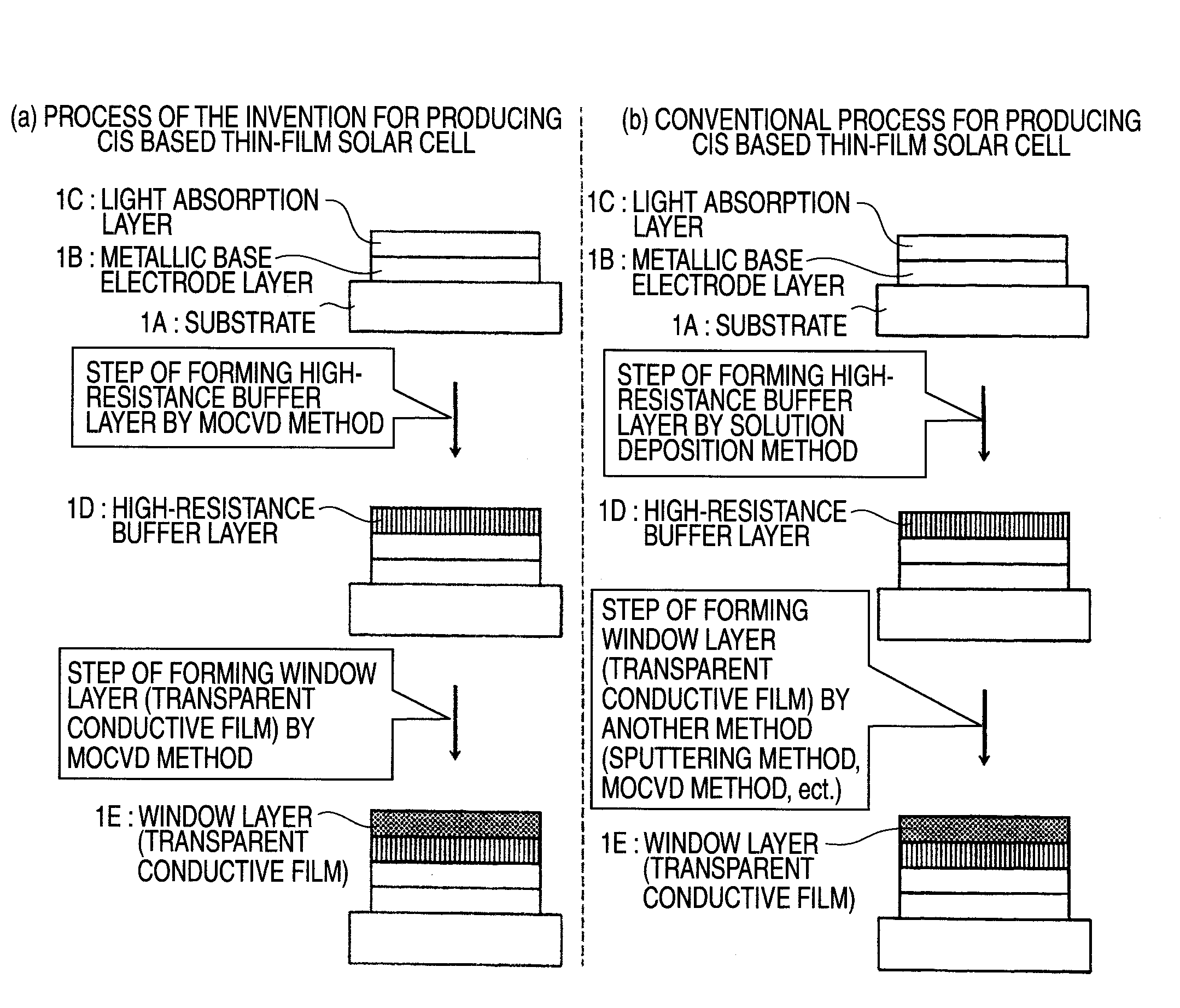
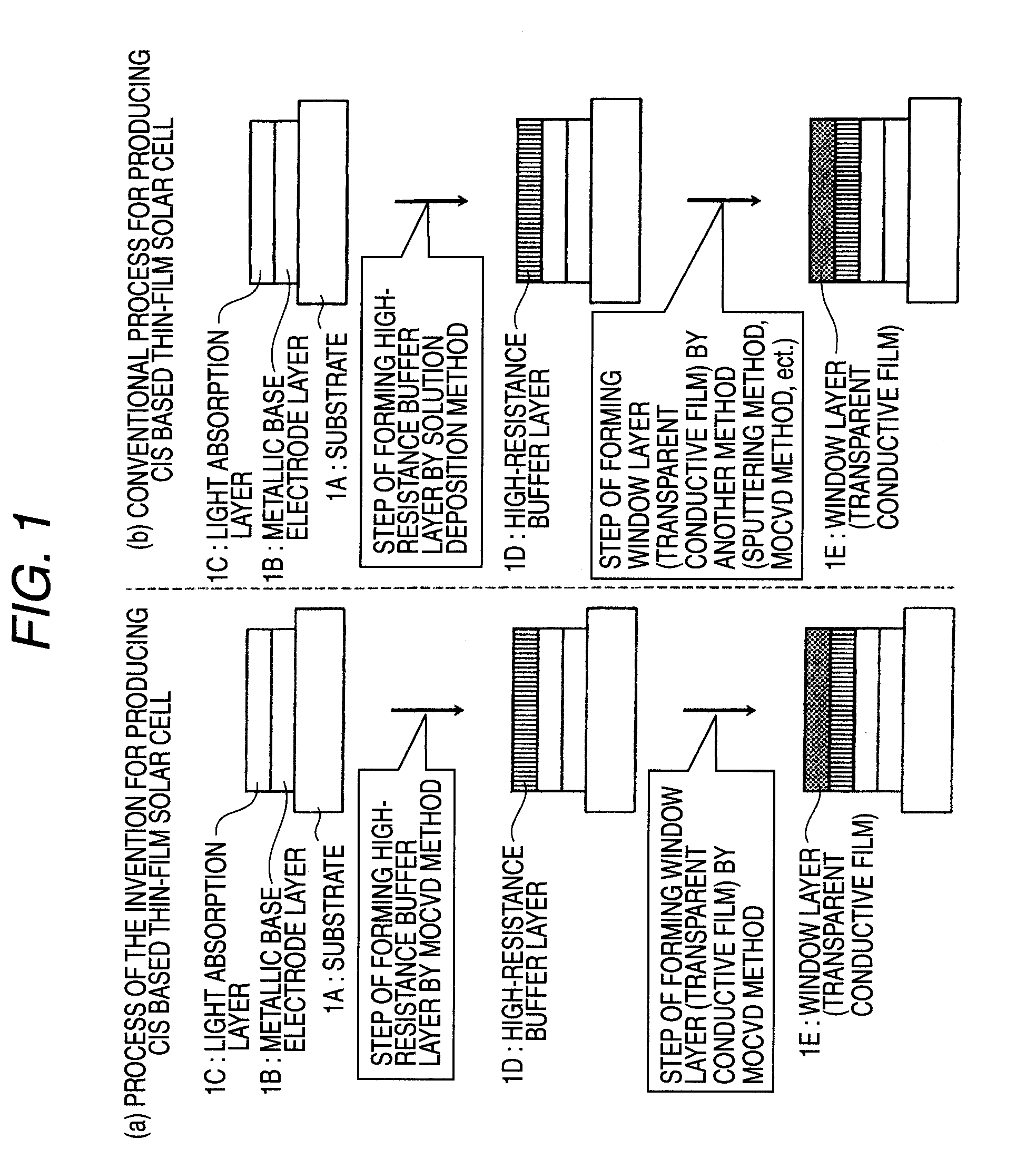
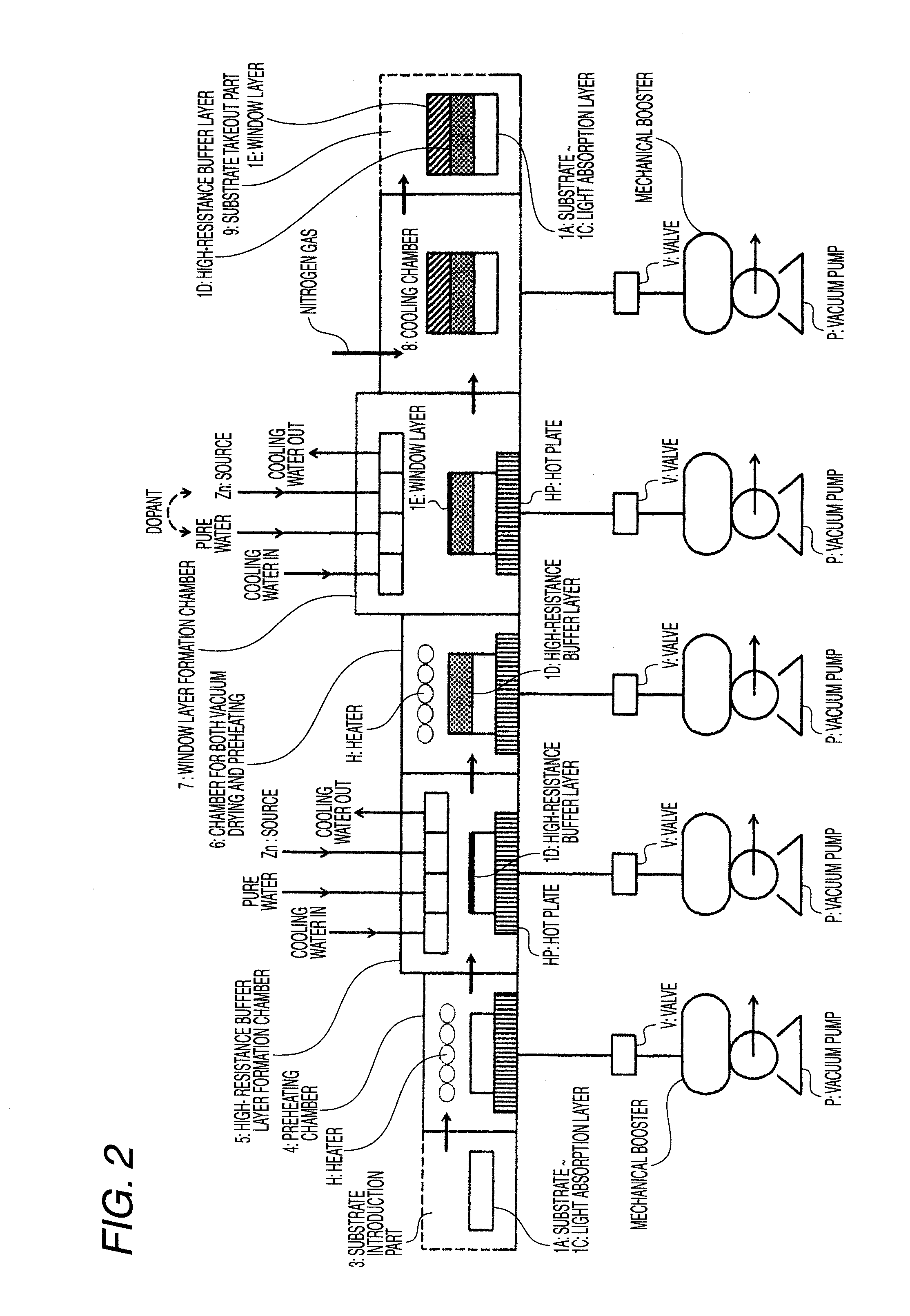
[0024]The invention relates to a method of successive high-resistance buffer layer / window layer (transparent conductive film) formation for a CIS based thin-film solar cell and an apparatus for successive film formation for carrying out the method of successive film formation.

[0025]As shown in FIG. 7, the CIS based thin-film solar cell is a pn heterojunction device of a substrate structure comprising a glass substrate 1A (thickness, 1-3 μm), a metallic base electrode layer 1B (a metal such as molybdenum or titanium having a thickness of 1-2 μm), a p-type CIS light absorption layer 1C, a high-resistance buffer layer 1D, and an n-type window layer (transparent conductive film) 1E which have been superposed in this order. The light absorption layer is a thin film which has a thickness of 1-3 μm and has a Cu-III-VI2 Group chalcopyrite structure having p-type conductivity. For example, it is a thin film o...


PUM

PropertyMeasurementUnit
thicknessaaaaaaaaaa
temperatureaaaaaaaaaa

Abstract

A high-resistance buffer layer and a window layer (transparent conductive film) are successively formed by the MOCVD method to obtain the same output characteristics as in conventional film deposition by the solution deposition method and to simplify a film deposition method and apparatus. Thus, the cost of raw materials and the cost of waste treatments are reduced to attain a considerable reduction in production cost.
After a metallic base electrode layer 1B and a light absorption layer 1C are formed in this order on a glass substrate 1A, a high-resistance buffer layer 1D and a window layer 1E are successively formed in this order in a multi layer arrangement on the light absorption layer 1C of the resultant semifinished solar cell substrate by the MOCVD method. Consequently, a film deposition method and apparatus are simplified and the cost of raw materials and the cost of waste treatments can be reduced.

Description

TECHNICAL FIELD[0001]The present invention relates to a method of successive film formation in which the high-resistance buffer layer and window layer (transparent conductive film) of a CIS based thin-film solar cell are successively formed by the MOCVD method and to an apparatus for successive film formation for carrying out the method of successive film formation.BACKGROUND ART[0002]CIS based thin-film solar cells were regarded as practically usable extensively. Patent document 1 among many publications discloses that to deposit a cadmium sulfide (CdS) layer as a high-resistance buffer layer on a light absorption layer comprising a thin CuInSe2 film is necessary for obtaining a thin solar cell having a high conversion efficiency. There is a statement in patent document 1 to the effect that the solution deposition method described therein, in which a thin CdS film is deposited from a solution, has the following effect. The immersion of a thin CuInSe2 light absorption layer in the s...

Claims


Application Information

Patent Timeline
Patent Type & Authority Applications(United States)
IPC IPC(8): H01L31/18
CPCC23C16/306C23C16/54Y02E10/543H01L31/1884Y02E10/541H01L31/0322H01L31/18Y02P70/50H01L31/0445
Inventor KUSHIYA, KATSUMI
Owner SOLAR FRONTIER
Why Eureka
Try Eureka