Donor substrates, laser induced thermal imaging methods using donor substrates and methods of manufacturing organic light emitting display devices using donor substrates

a technology of laser induced thermal imaging and donor substrates, which is applied in thermoelectric devices, basic electric elements, and final product manufacturing. it can solve the problems of thermal energy damage to the transfer layer or the display substrate of the hard application of the deposition process to the organic light emitting display device having a relatively large area, so as to reduce the excess thermal transfer and small thermal conductivity

Active Publication Date: 2013-12-26
SAMSUNG DISPLAY CO LTD
View PDF3 Cites 7 Cited by
  • Summary
  • Abstract
  • Description
  • Claims
  • Application Information

AI Technical Summary

Benefits of technology

[0024]According to example embodiments, a buffer layer may include at least one porous layer that may include a plurality of pores. The pores may have a relatively small thermal conductivity, so that the buffer layer may reduce an excess thermal transfer from a light to heat conversion layer to a transfer layer. Therefore, the transfer and / or the substrate (to which the organic layer pattern may be transferred) may not be damaged by the thermal energy. Further, the buffer layer may include the intermediate layer that may prevent the transfer layer from being deteriorated by the harmful gas or the impurities.

Problems solved by technology

When using a deposition process for forming organic layers, it may be hard to apply the deposition process to the organic light emitting display device having a relatively large area, because the deposition process may use a micro-dimensioned metal mask.
As for the conventional laser induced thermal imaging process, however, the thermal energy may damage the transfer layer or the display substrate of the organic light emitting display device.

Method used


Image

  • Donor substrates, laser induced thermal imaging methods using donor substrates and methods of manufacturing organic light emitting display devices using donor substrates
  • Donor substrates, laser induced thermal imaging methods using donor substrates and methods of manufacturing organic light emitting display devices using donor substrates
  • Donor substrates, laser induced thermal imaging methods using donor substrates and methods of manufacturing organic light emitting display devices using donor substrates

Examples


Embodiment Construction

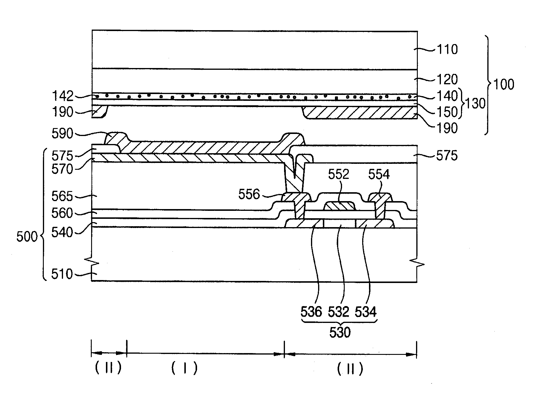
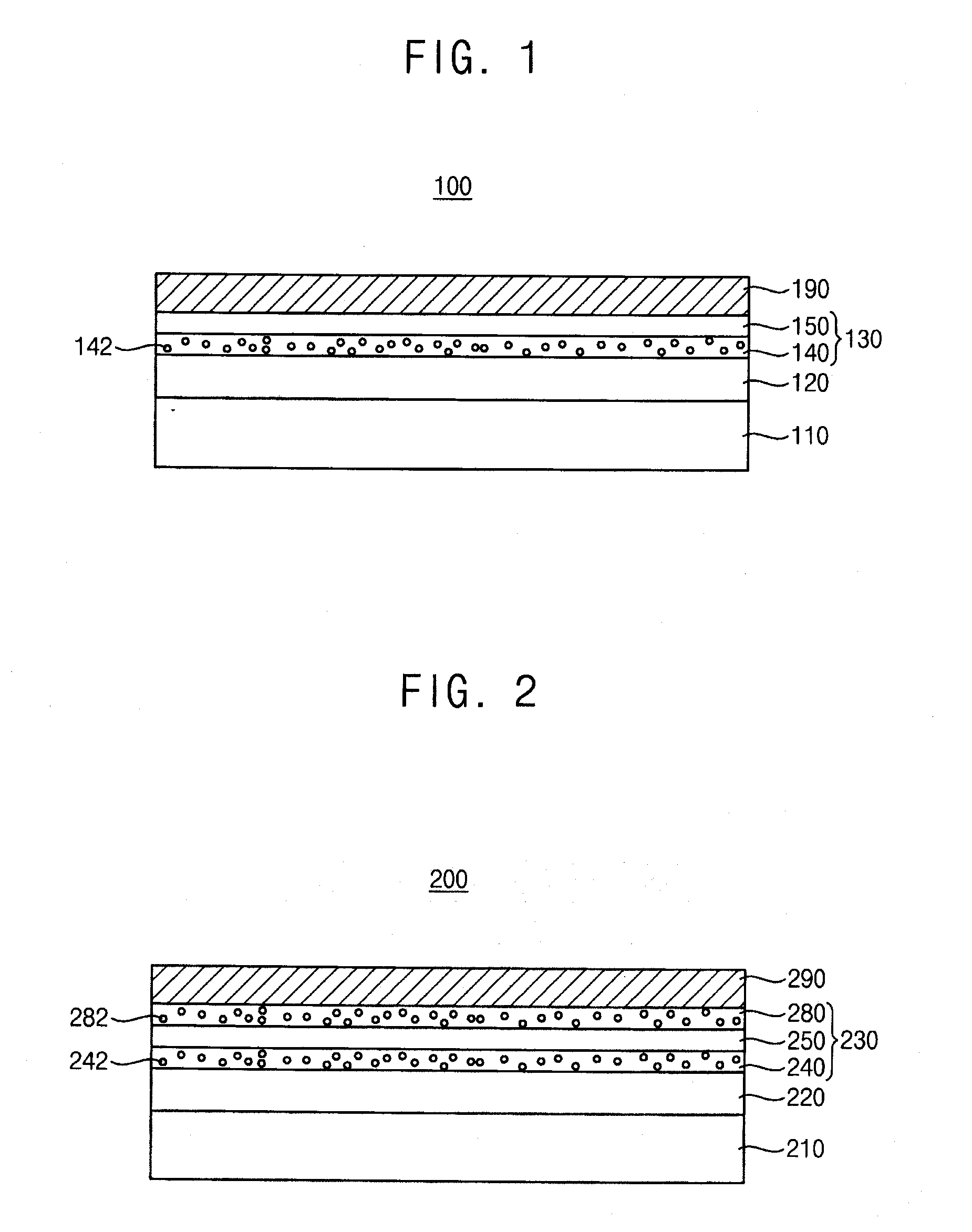
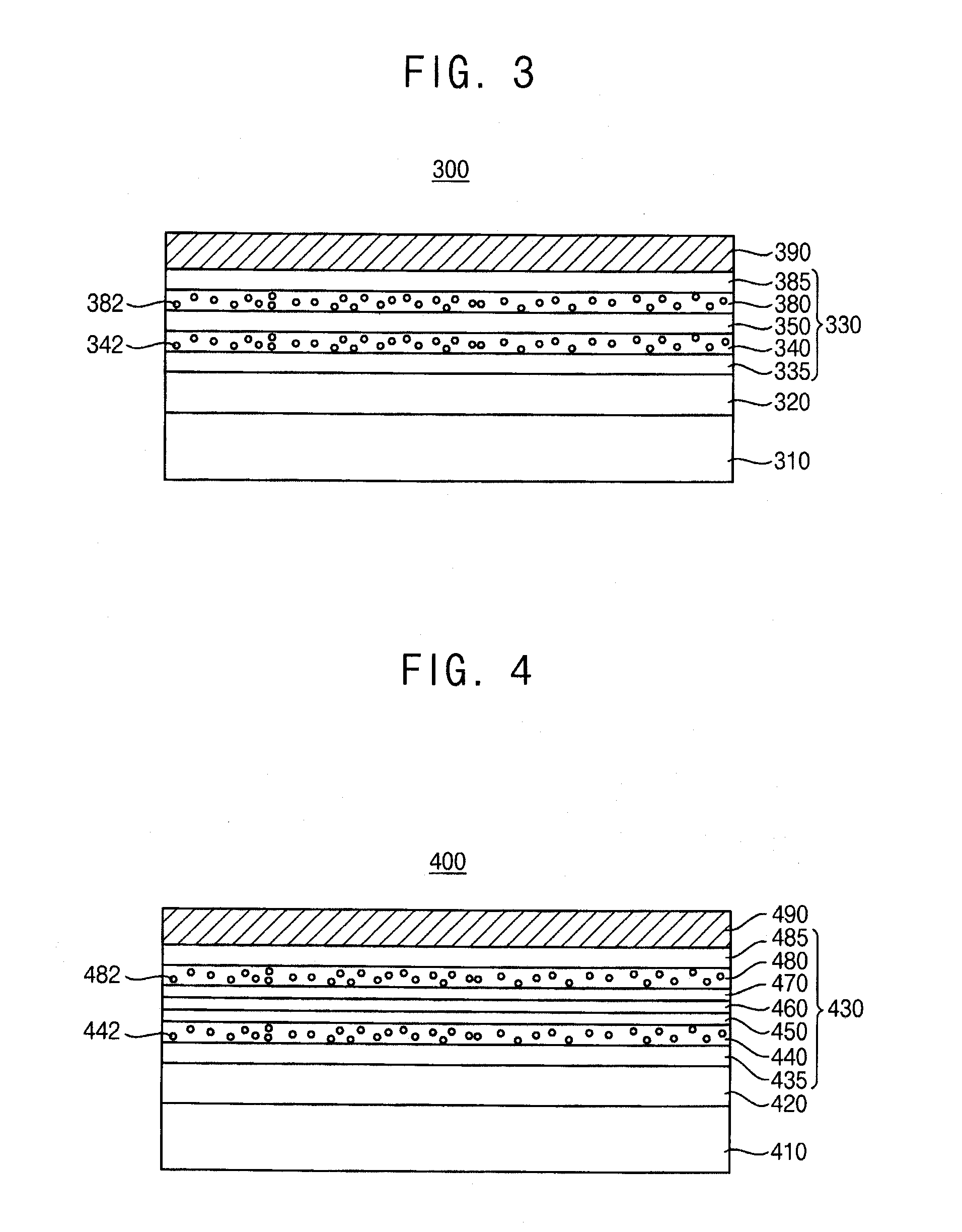
[0032]Various embodiments will be described more fully hereinafter with reference to the accompanying drawings, in which some embodiments are shown. The present embodiments may, however, be embodied in many different forms and should not be construed as limited to the embodiments set forth herein. Rather, these embodiments are provided so that this description will be thorough and complete, and will fully convey the scope of the present embodiments to those skilled in the art. In the drawings, the sizes and relative sizes of layers and regions may be exaggerated for clarity.

[0033]It will be understood that when an element or layer is referred to as being “on,”“connected to” or “coupled to” another element or layer, it can be directly on, connected or coupled to the other element or layer or intervening elements or layers may be present. In contrast, when an element is referred to as being “directly on,”“directly connected to” or “directly coupled to” another element or layer, there ...


PUM


Abstract

A donor substrate includes a base substrate, a light to heat conversion layer, a buffer layer and a transfer layer. The light to heat conversion layer may be disposed on the base substrate. The buffer layer may be disposed on the light to heat conversion layer. The buffer layer may include at least one porous layer having a plurality of pores. The transfer layer may be disposed on the buffer layer.

Description

CROSS-REFERENCE TO RELATED APPLICATIONS[0001]This application claims priority under 35 USC §119 to Korean Patent Application No. 10-2012-0068027 filed on Jun. 25, 2012 in the Korean Intellectual Property Office (KIPO), the contents of which are herein incorporated by reference in its entirety.BACKGROUND[0002]1. Field[0003]Example embodiments relate to donor substrates, laser induced thermal imaging method using donor substrates and methods of manufacturing organic light emitting display devices using donor substrates. More particularly, example embodiments relate to donor substrates including buffer layers, laser induced thermal imaging methods using donor substrates including buffer layers and methods of manufacturing organic light emitting display devices using donor substrates including buffer layers.[0004]2. Description of the Related Art[0005]Generally, organic light emitting display devices may include various organic layers such as an organic light emitting layer, a hole inje...

Claims


Application Information

Patent Timeline
Patent Type & Authority Applications(United States)
IPC IPC(8): H01L51/52H01L51/56
CPCH01L51/529H01L51/56H10K71/80H10K71/00Y02E10/549Y02P70/50H10K71/18H10K59/12H10K77/10H10K50/87
Inventor PYO, SANG-WOOSONG, HA-JINYOO, BYEONG-WOOKKIM, HYO-YEONLEE, KWAN-HEE
Owner SAMSUNG DISPLAY CO LTD
Why Eureka
Try Eureka