
Ultra-wideband extremely low profile wide angle scanning phased array with compact balun and feed structure

Active Publication Date: 2014-01-09
THE OHIO STATES UNIV
View PDF4 Cites 7 Cited by
  • Summary
  • Abstract
  • Description
  • Claims
  • Application Information

AI Technical Summary

Benefits of technology

The patent is about a new design for a tightly coupled dipole array (TCDA) that solves problems of size and weight limitations in current designs. The new design uses a compact Marchand balun as an impedance matching network for each feed port, which eliminates the need for external baluns while improving bandwidth and minimizing cross-polarization. The balun / impedance matching network can be printed on the same substrate as the array, making it a highly compact and low-cost wideband electronically scanned array (ESA). The overall size, weight, and cost of the array are reduced, and bandwidth is improved compared to other feeding techniques.

Problems solved by technology

The volume available for such a balun is limited, particularly for designs capable of operating at frequencies above 500 MHz.
As a result, the known art has not been able to obtain a compact antenna array with a small or low profile and desired performance.
Known TCDA designs use bulky external baluns or hybrids located below the ground plane of the TCDA structure, significantly increasing the total size, weight, and cost of the array.
Practical implementation of a wideband balun that physically fits within this available volume has been a problem, and known designs which physically fit within this available space yield bandwidths of less than 2:1.
An alternative technique, as described in U.S published patent application number 2012 / 0146869, forgoes baluns altogether and uses vias to mitigate common mode resonances, resulting in 3:1 bandwidth or 5:1 bandwidth with additional external baluns or hybrids located below the ground plane, significantly increasing the total size, weight, and cost of the array.

Method used


Image

  • Ultra-wideband extremely low profile wide angle scanning phased array with compact balun and feed structure
  • Ultra-wideband extremely low profile wide angle scanning phased array with compact balun and feed structure
  • Ultra-wideband extremely low profile wide angle scanning phased array with compact balun and feed structure

Examples


Embodiment Construction

)

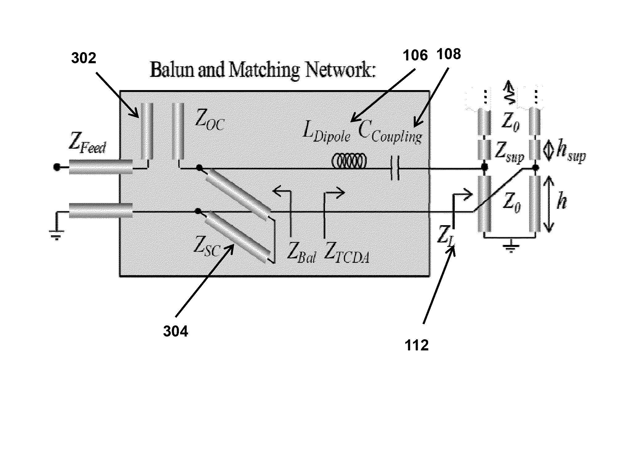
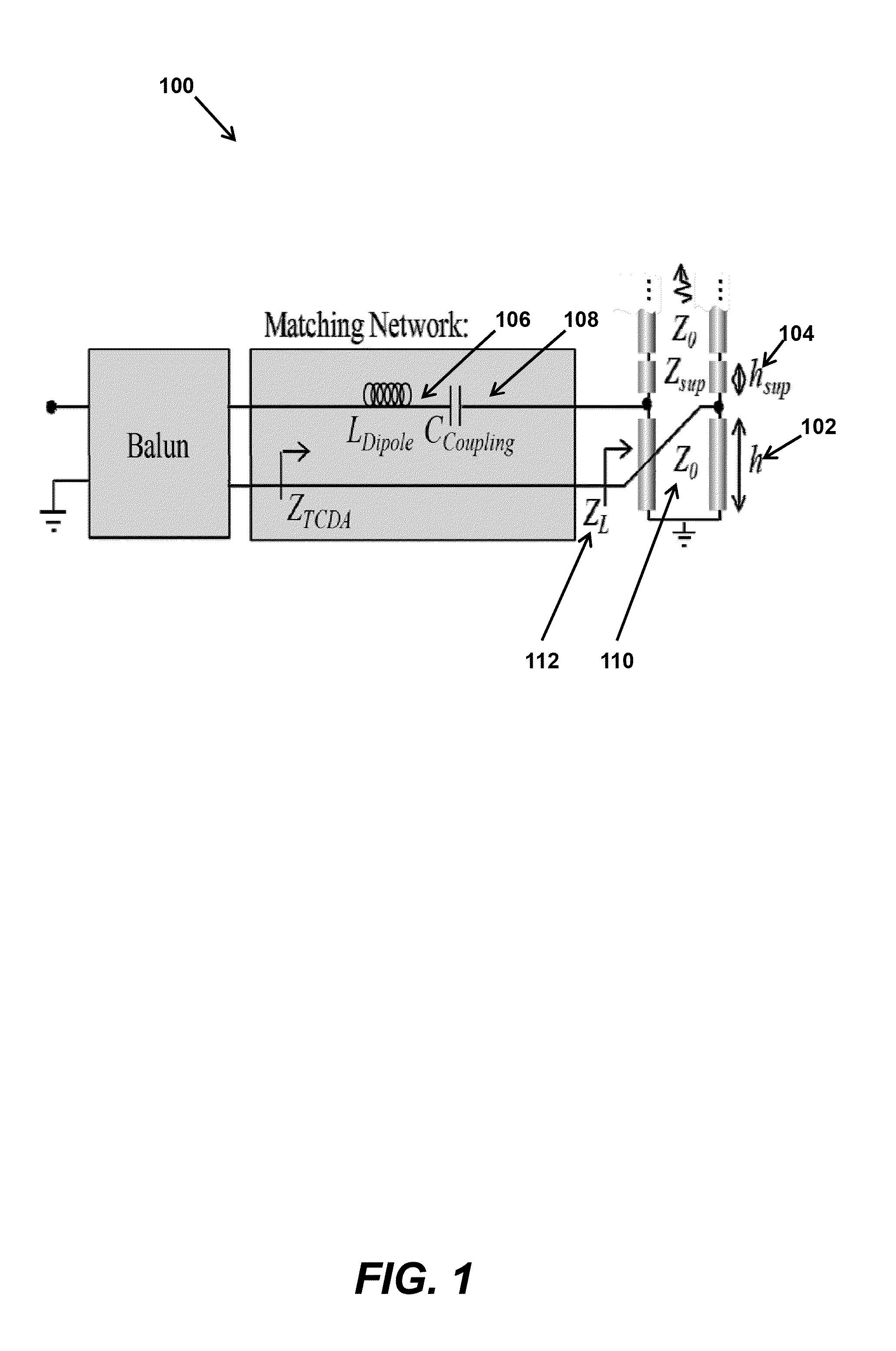
[0020]Exemplary embodiments of the present invention are directed to networks for use with a wideband scanning array antenna and the associated wideband scanning array antenna structures. Such networks may function both as balun and impedance matching networks while simultaneously improving the array bandwidth and providing a 50 ohm unbalanced feed for each element of the array. Other embodiments may be configured to provide unbalanced feeds with impedances in the range of about 25-200 ohm.

[0021]Electrically-small baluns of known designs may exhibit large reactive impedances, limiting their overall bandwidth when implemented. The inventors have discovered that the intrinsic reactance of electrically small Marchand-type baluns may be configured as an impedance matching network to compensate for the reactance of the antenna load and improve the bandwidth of TCDA-type phased arrays. The result may be an incorporation of the balun into the matching network, forming a higher order match...


PUM

PropertyMeasurementUnit
Electrical resistanceaaaaaaaaaa
Heightaaaaaaaaaa
Electric impedanceaaaaaaaaaa

Abstract

A phased array antenna comprising a dielectric superstrate material, a ground plane material, a plurality of dipole structures located between the superstrate and ground plane materials, and a plurality of balun and matching networks in electrical communication with the plurality of dipole structures, wherein the phased array antenna is adapted to achieve a bandwidth of at least about 7:1.

Description

CROSS-REFERENCE TO RELATED APPLICATIONS[0001]This application claims priority to provisional patent application 61 / 669,377, filed Jul. 9, 2012, which is hereby incorporated by reference in its entirety.[0002]This invention was made with government support under contract no. N68936-09-C-0099 awarded by Naval Air Systems Command. The government may have certain rights in the invention.BACKGROUND AND SUMMARY OF THE INVENTION[0003]Exemplary embodiments of the present invention relate generally to compact scanning phased array antenna devices.[0004]Tightly Coupled Dipole Arrays (TCDAs) are frequently implemented as a result of their low profile, bandwidths up to 6:1, good scan performance, and low cross polarization characteristics. However, the dipole elements used in TCDAs are balanced structures, and as a result, the feed network for a TCDA must include baluns or 180° hybrids that can sustain array bandwidths of greater than 6:1.[0005]The volume available for such a balun is limited, ...

Claims


Application Information

Patent Timeline
IPC IPC(8): H01Q21/00
CPCH01Q21/0006H01Q21/0087H01Q21/062Y10T29/49016
Inventor SERTEL, KUBILAYDOANE, JONATHAN
Owner THE OHIO STATES UNIV
Learn More