Wafer Inspection

a technology of water filter and water filter, which is applied in the direction of optical radiation measurement, semiconductor/solid-state device testing/measurement, instruments, etc., can solve the problems of difficult reconfiguration to optimize the system for different samples and defects, and the segmentation of the na is fixed, so as to minimize the detection of scattering, maximize collection and detection of scattering, and minimize the effect of particle detection

Active Publication Date: 2014-01-09
KLA CORP
View PDF4 Cites 35 Cited by
  • Summary
  • Abstract
  • Description
  • Claims
  • Application Information

AI Technical Summary

Benefits of technology

[0021]As described further herein, one detector included in the system may be optimized for substantially high sensitivity to particles by optimizing the polarization and one or more characteristics (e.g., shape) of the segment of the collection NA detected by the detector such that the scattering from the wafer surface and, at the same time, the loss of scattering from particles are minimized thereby maximizing the signal-to-noise ratio of the particles. Other detectors may be optimized for substantially high sensitivity to other defect types such as scratches, pits, and stains in a similar manner (e.g., by configuring the polarization of the scattered light and the characteristic(s) of the segments of the collection NA directed onto the corresponding detectors). Each of these embodiments of the system may be further configured as described herein.
[0023]Each of the steps of the method described above may be further performed as described herein. In addition, each of the steps of the method may be performed using any of the system(s) described herein. Furthermore, the method may include any other step(s) that can be performed by any of the system(s) described herein. For example, the collection subsystem used in the method may include polarization preserving collection optics that may be configured as described herein. In addition, separating the scattered light collected in different segments of the collection NA may include dividing the full collection NA into multiple detection channels. The optical element and the polarizing element used in the method may be configured to optimize detection of one of the different portions of the scattered light for high sensitivity to particles. Therefore, a system used to perform the method may include a detection channel that is optimized for high sensitivity to particles. For example, a shape of a segment of the collection NA for a particle sensitive detection channel and the polarization of the light detected by the particle sensitive detection channel may be configured to minimize detection of scattering from the wafer surface (noise) and maximize collection and detection of scattering from the particles (signal). Other channels included in a system configured to perform the method may be optimized for best sensitivity to other defect types in a similar manner.

Problems solved by technology

The disadvantages of the above-referenced systems can be described based on the similarities among the various inspection systems.
For example, for “hard-wired” segmentation of the collection NA (e.g., collection that uses multiple lens collectors to divide the hemisphere of scattering into multiple segments), one disadvantage that such systems have in common is that the segmentation of the NA is fixed and is therefore difficult to reconfigure to optimize the systems for different samples and defects.
In this manner, such configurations may have less than optimum performance for various defect types.
Another disadvantage of such systems is that the majority of the collector optics is at a tilted angle with respect to the wafer surface normal.
Therefore, it is difficult, if not impossible, to image multiple spots onto a detector array.
As such, these configurations are not compatible with multi-spot illumination.
In addition, the collection is also less efficient due to gaps between collectors.
For mirror-based, large NA collection (e.g., collection that uses a single large NA collector that is based on a mirror, e.g., ellipsoidal or parabolic), the disadvantage of using a mirror collector is that the polarization changes upon reflection due to the substantially large phase shift between p and s polarization.
This effect scrambles the well-aligned nearly linear polarization of surface scattering from smooth silicon wafer surfaces, making it substantially difficult to use a polarizer to suppress the surface scattering and therefore undermines a capability to improve defect sensitivity.
There are two disadvantages to this approach: 1) the collection hemisphere is divided into multiple separate collection solid angles rendering the system complex and the collection efficiency low; and 2) the polarization of scattered light is mapped onto the surface of a hemisphere, across which the polarization of scattered light changes with scattering angle.
This second disadvantage is the main reason that in previously used systems the hemisphere has to be divided up (so that over each relatively small aperture, the polarization of surface scattering is approximately aligned).
For example, the spacing in the radial direction between spots needs to change when the spot size changes, which can result in pitch changes between tracks.

Method used


Image

  • Wafer Inspection
  • Wafer Inspection
  • Wafer Inspection

Examples


Embodiment Construction

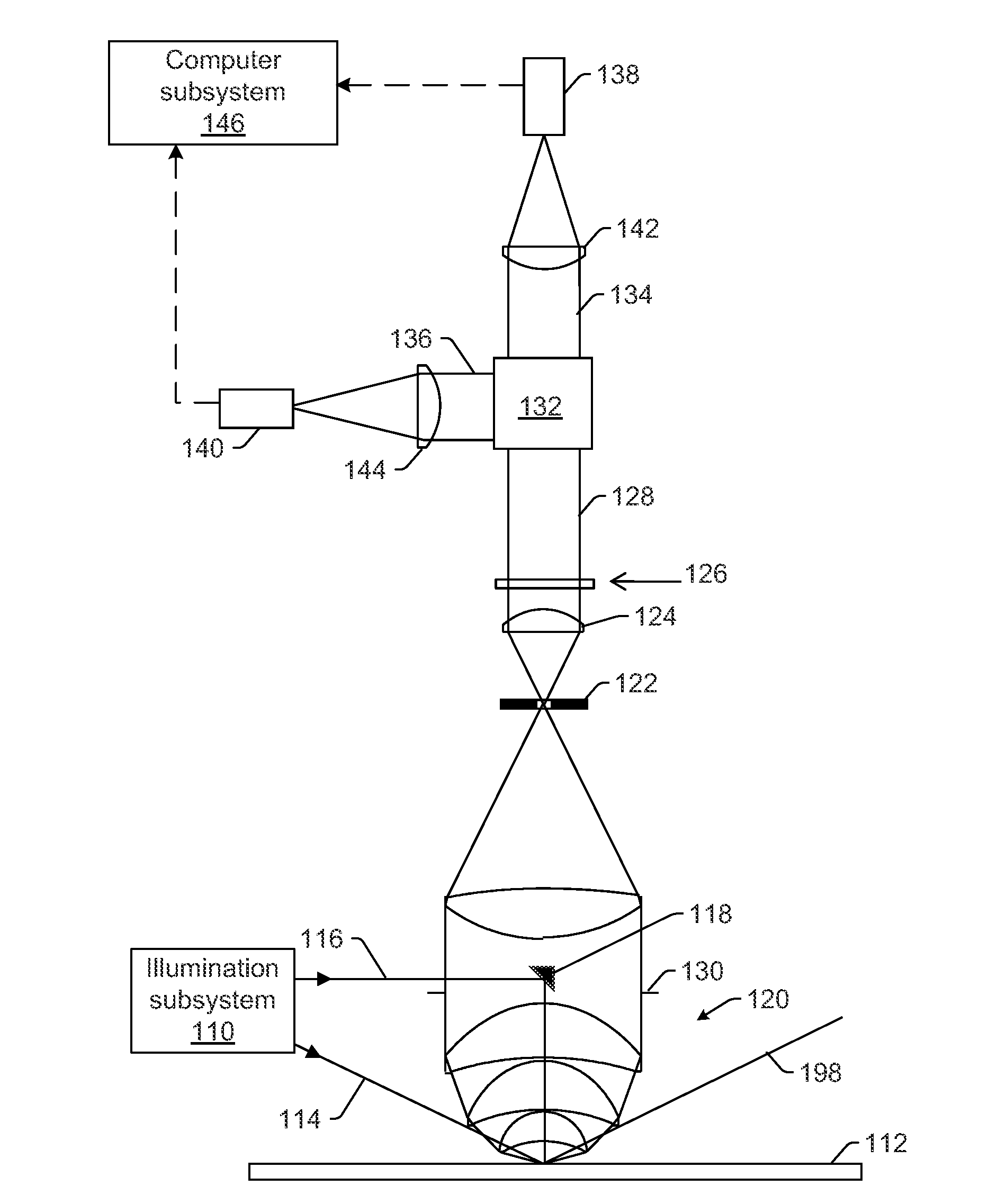
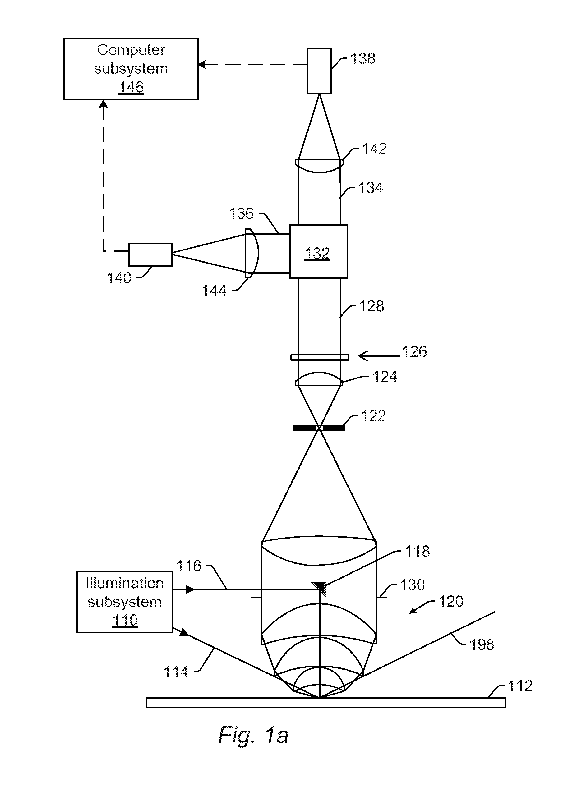
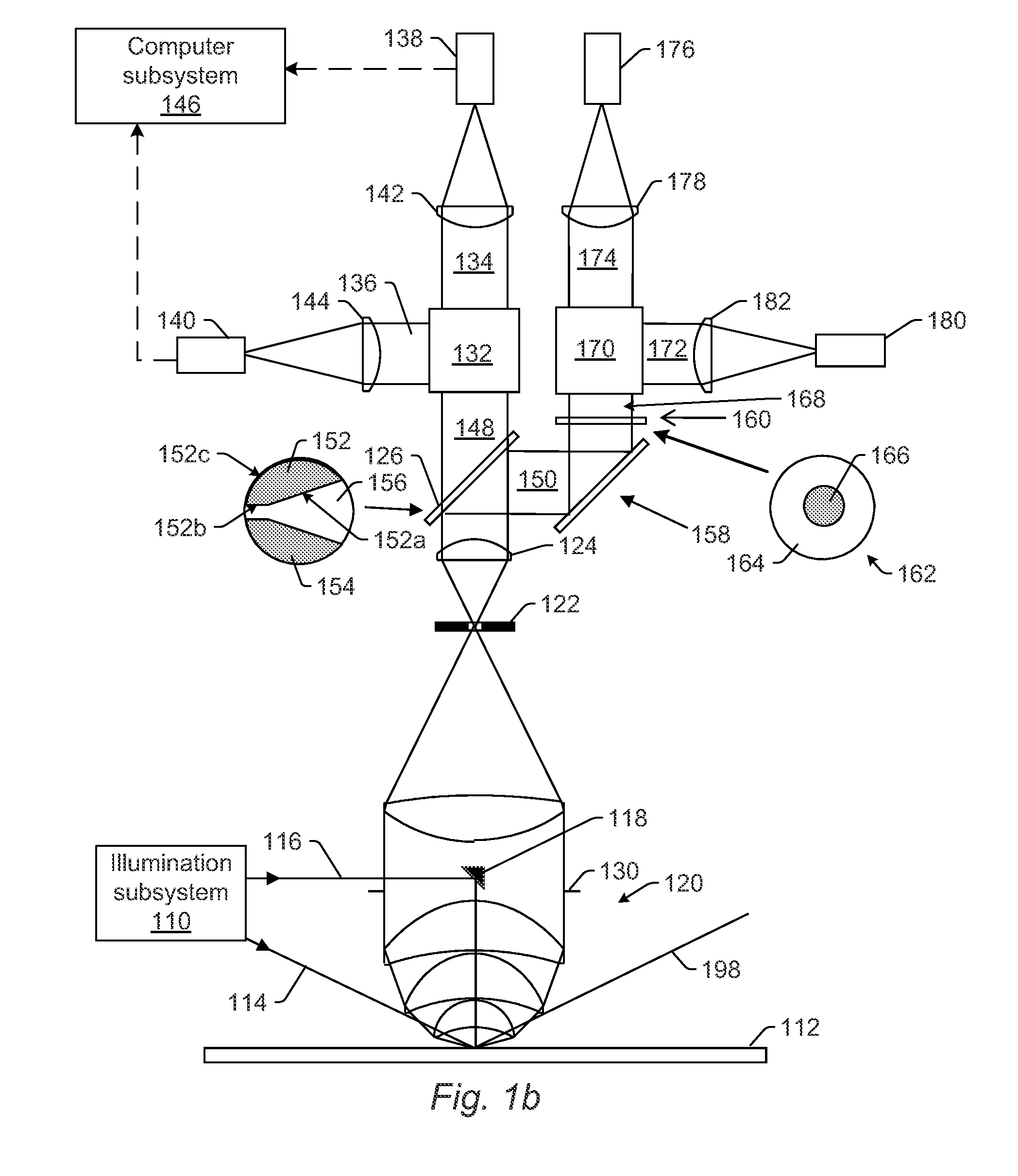
[0038]Turning now to the drawings, it is noted that the figures are not drawn to scale. In particular, the scale of some of the elements of the figures is greatly exaggerated to emphasize characteristics of the elements. It is also noted that the figures are not drawn to the same scale. Elements shown in more than one figure that may be similarly configured have been indicated using the same reference numerals.

[0039]FIG. 1a illustrates one embodiment of a system configured to inspect a wafer. The system includes an illumination subsystem configured to illuminate the wafer. For example, illumination subsystem 110 may be configured to illuminate wafer 112 by directing oblique illumination 114 to the wafer and / or normal illumination 116 to the wafer. For example, the illumination subsystem may include a number of optical elements such as reflective optical element 118 configured to direct light from one or more light sources (not shown) to the wafer at one or more desired angles of inc...


PUM

PropertyMeasurementUnit
wavelengthaaaaaaaaaa

Abstract

Systems and methods for inspecting a wafer are provided. One system includes an illumination subsystem configured to illuminate the wafer; a collection subsystem configured to collect light scattered from the wafer and to preserve the polarization of the scattered light; an optical element configured to separate the scattered light collected in different segments of the collection numerical aperture of the collection subsystem, where the optical element is positioned at a Fourier plane or a conjugate of the Fourier plane of the collection subsystem; a polarizing element configured to separate the scattered light in one of the different segments into different portions of the scattered light based on polarization; and a detector configured to detect one of the different. portions of the scattered light and to generate output responsive to the detected light, which is used to detect defects on the wafer.

Description

BACKGROUND OF THE INVENTION[0001]1. Field of the Invention[0002]This invention generally relates to systems and methods for inspecting a water. Certain embodiments relate to a wafer inspection system that can include various optical elements and polarizing elements, which in combination segment the collection numerical aperture of a collection subsystem thereby optimizing the system for detection of certain defects while also possibly suppressing detection of other defects.[0003]2. Description of the Related Art[0004]The following description and examples are not admitted to be prior art by virtue of their inclusion in this section.[0005]Examples of commercially available wafer inspection systems include the Surfscan SP1, SP2, and SP3 systems, which are commercially available from KLA-Tencor, Milpitas, Calif., and which generally are single-spot, spiral-scanning systems using an ellipsoidal collector and a supplementary small lens collector that fills in the central numerical apertu...

Claims


Application Information

Patent Timeline
Patent Type & Authority Applications(United States)
IPC IPC(8): G01N21/88
CPCG01N21/8806H01L22/12H01L2924/0002G01N21/9501H01L2924/00H01L22/00G01N21/21G01N21/47G01N2201/06113
Inventor ZHAO, GUOHENGLEONG, JENN-KUENVAEZ-IRAVANI, MEHDI
Owner KLA CORP
Why Eureka
Try Eureka