

Surface emitting laser device and atomic oscillator
a laser device and laser technology, applied in semiconductor lasers, instruments, horology, etc., can solve the problems of insufficient laser performance and increase electrical resistance, and achieve the effect of uniform electrical resistance and desirable wavelength controllability
- Summary
- Abstract
- Description
- Claims
- Application Information
AI Technical Summary
Benefits of technology
Problems solved by technology
Method used
Image

Examples
first embodiment
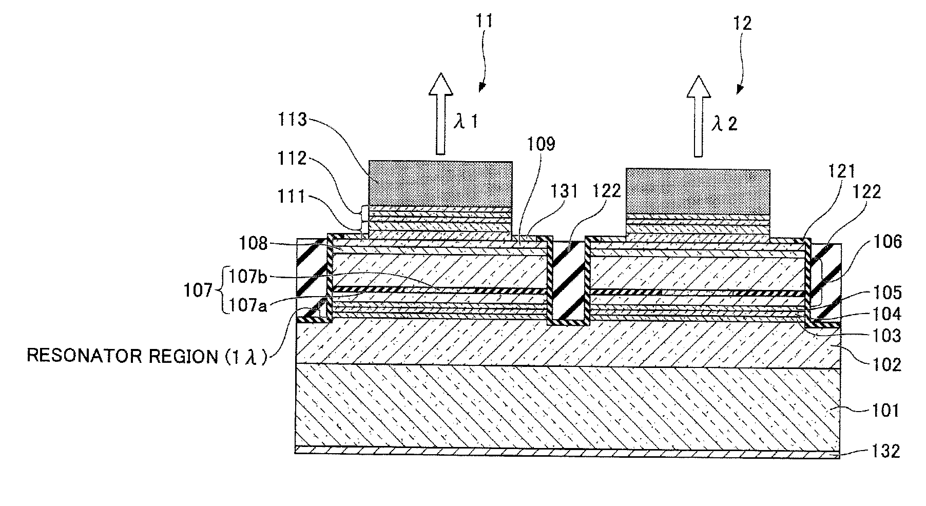
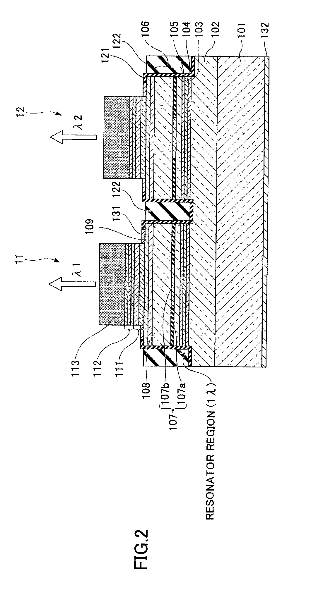
[0045]In the following, a surface emitting laser device according to a first embodiment of the present invention is described with reference to FIGS. 1-3. The surface emitting laser device of the present embodiment is for emitting light at an oscillation wavelength in the 894.6 nm range.
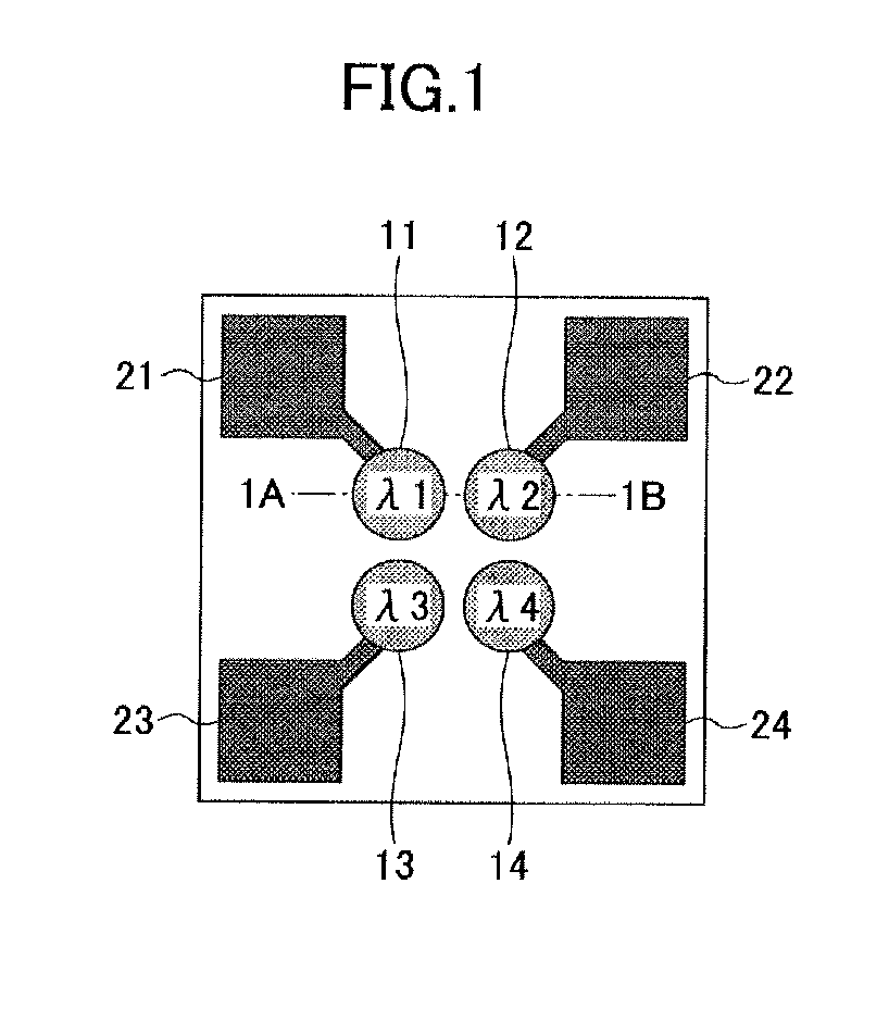
[0046]The surface emitting laser device illustrated in FIG. 1 corresponds to a semiconductor device that has four surface emitting lasers 11, 12, 13, and 14 formed on a 300 μm square semiconductor chip. FIG. 2 is a cross-sectional view of the surface emitting laser device along dot-dashed line 1A-1B of FIG. 1. Although not shown in FIG. 1, the surface emitting lasers 11, 12, 13, and 14 each have upper electrodes arranged thereon. The upper electrode of the surface emitting laser 11 is connected to electrode pad 21, the upper electrode of the surface emitting laser 12 is connected to electrode pad 22, the upper electrode of the surface emitting laser 13 is connected to electrode pad 23, and the upper ...
second embodiment
[0079]In the following, a surface emitting laser device according to a second embodiment of the present invention is described. The surface emitting laser device of the present embodiment is for emitting light at an oscillation wavelength of 894.6 nm. As described above, in the surface emitting laser device of the first embodiment, the layer 140 including the wavelength adjustment layer 112 is arranged to replace one of the high refractive index layers of the second upper reflector 106. In the surface emitting laser device of the present embodiment, a layer including a wavelength adjustment layer replaces a low refractive layer. Specifically, as illustrated in FIG. 9B, in the surface emitting laser device of the present embodiment, a layer 240 including a wavelength adjustment layer 212 is made of a low refractive index material, and the total optical thickness of the layer 240 including the wavelength adjustment layer 212 and a low refractive index layer of a dielectric multi-layer...
third embodiment
[0111]In the following, a surface emitting laser device according to a third embodiment of the present invention is described. The surface emitting laser device of the present embodiment is for emitting light at an oscillation wavelength in the 894.6 nm range.
[0112]FIG. 17 is a cross-sectional view of the surface emitting laser device of the present embodiment. Note that the top view of the surface emitting laser device of the present embodiment may be identical to that of the first embodiment as illustrated in FIG. 1. The surface emitting laser device of the present embodiment includes the substrate 101 made of a semiconductor material on which the lower reflector 102, the lower spacer layer 103, the active layer 104, the upper spacer layer 105, the current confinement layer 107, the second phase adjustment layer 108, the contact layer 109, the first phase adjustment layer 111, the wavelength adjustment layer 112, and an upper reflector 213 are layered. Also, mesas are formed by pa...
PUM
 Abstract
Description
Claims
Application Information