

Data writing method, and memory controller and memory storage apparatus using the same
a data writing and memory controller technology, applied in the direction of digital storage, memory adressing/allocation/relocation, instruments, etc., can solve problems such as errors, and achieve the effect of reducing the occurrence of errors and effectively preventing over-programming
- Summary
- Abstract
- Description
- Claims
- Application Information
AI Technical Summary
Benefits of technology
Problems solved by technology
Method used
Image

Examples
first exemplary embodiment
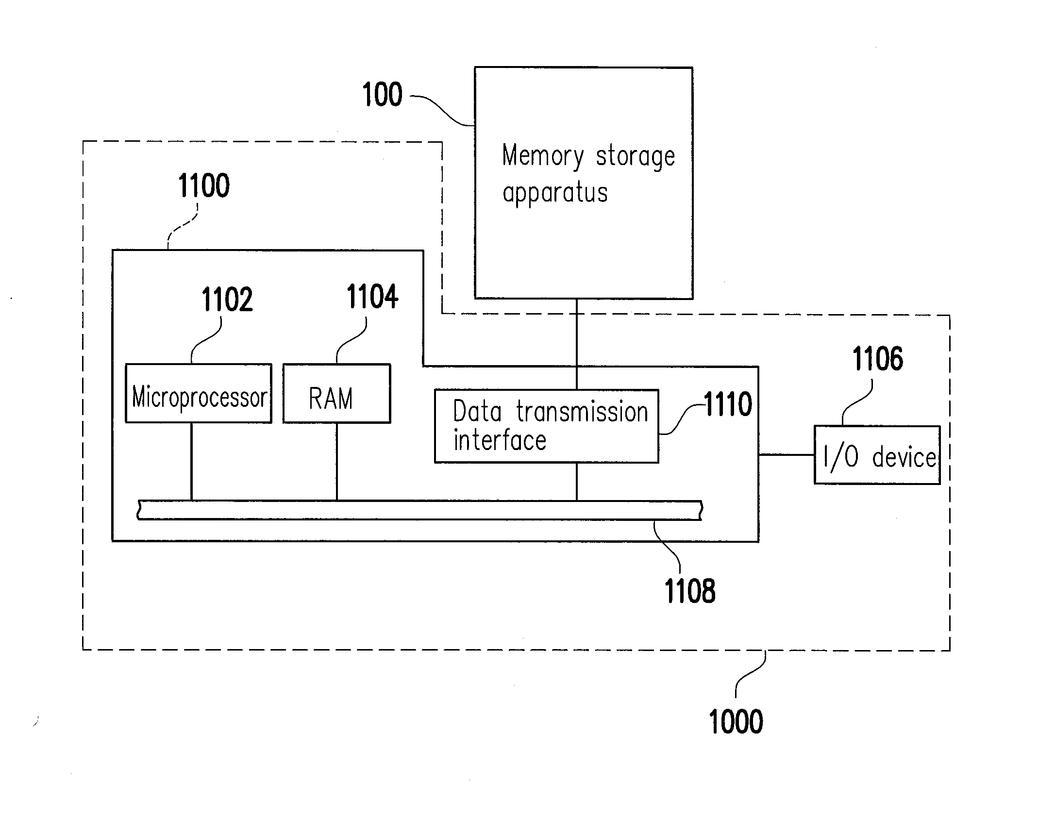
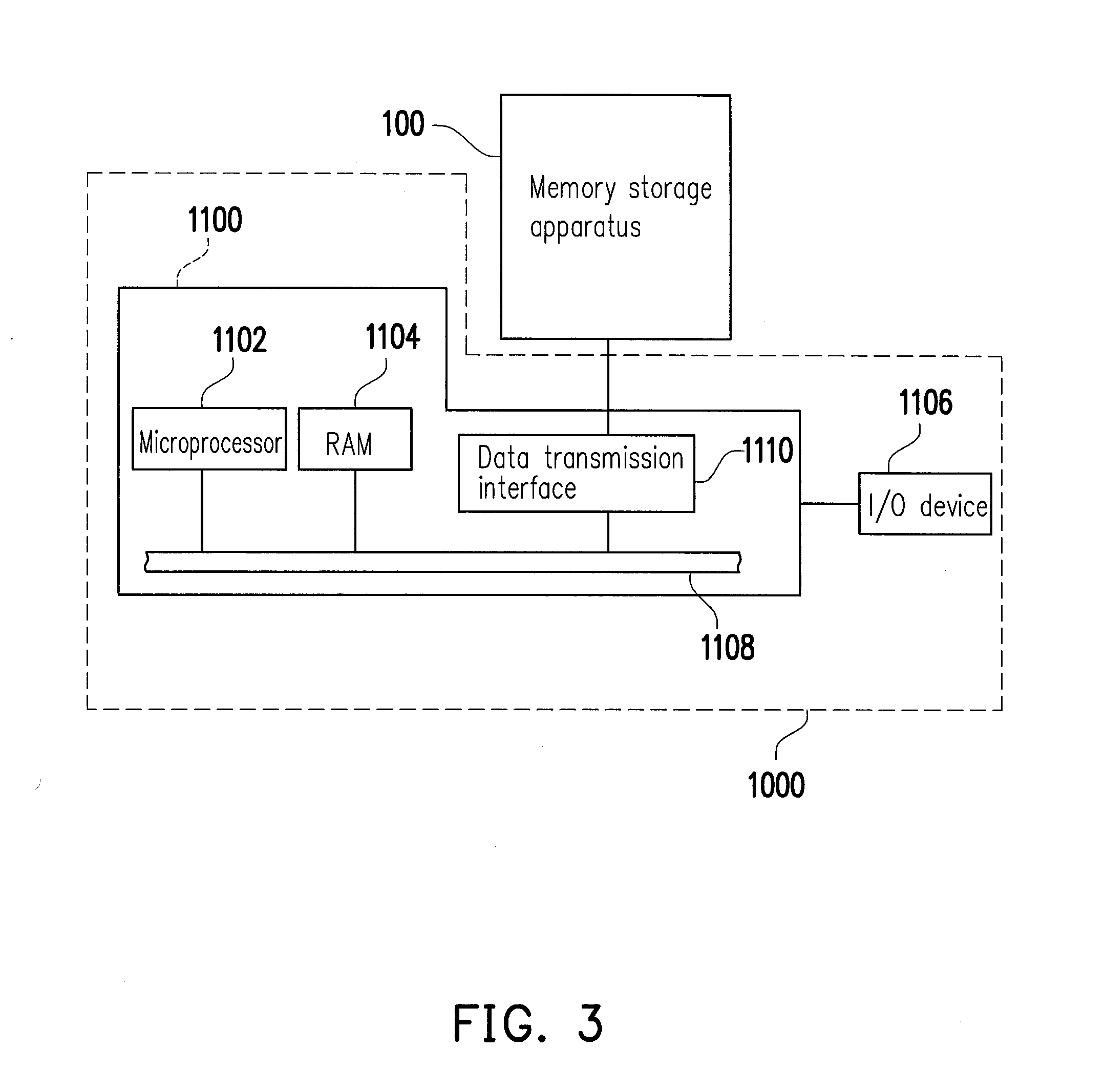
[0041]A memory storage apparatus (i.e., a memory storage system) typically includes a rewritable non-volatile memory module and a controller (i.e., a control circuit). The memory storage apparatus is usually used together with a host system, such that the host system can write data into or read data from the memory storage apparatus.
[0042]FIG. 3 illustrates a host system and a memory storage apparatus according to a first exemplary embodiment of the present invention.
[0043]Referring to FIG. 3, a host system 1000 includes a computer 1100 and an input / output (I / O) device 1106. The computer 1100 includes a microprocessor 1102, a random access memory (RAM) 1104, a system bus 1108, and a data transmission interface 1110. The I / O device 1106 includes a mouse 1202, a keyboard 1204, a display 1206, and a printer 1208 as shown in FIG. 4. It should be understood that the I / O device 1106 is not limited to the devices illustrated in FIG. 4 and may further include other devices.
[0044]In the exem...
second exemplary embodiment
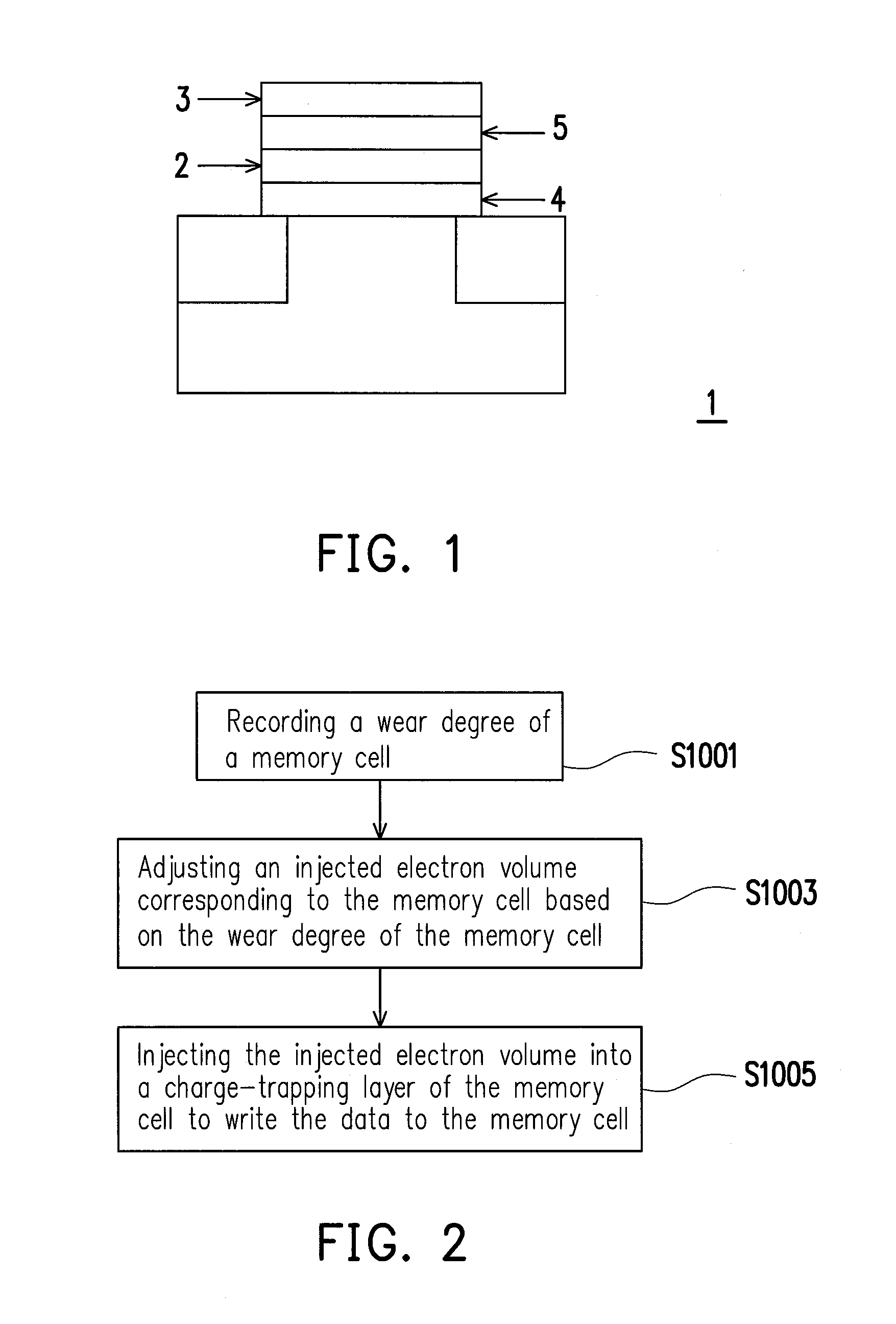
[0099]The second exemplary embodiment illustrates a structure of a memory storage apparatus similar to the memory storage apparatus of the first exemplary embodiment, and the difference therebetween is that a memory controller (or a memory management circuit) of the second exemplary embodiment adjusts an electron volume contained in a charge-trapping layer by adjusting a write voltage pulse time applied during programming based on a wear degree of each memory cell, so that error bits caused by over-writing are prevented. The difference between the second exemplary embodiment and the first exemplary embodiment will be described by using the same symbols used in the first exemplary embodiment.
[0100]Typically, the memory controller 104 (or the memory management circuit 202) applies a preset time (e.g. 16 μs) as the write voltage pulse time corresponding to the memory cell of the rewritable non-volatile memory module (e.g. a flash memory module) 106. Meanwhile, during programming the me...
PUM
 Abstract
Description
Claims
Application Information