Semiconductor device and method of manufacturing the same

a technology of semiconductor devices and semiconductors, applied in semiconductor devices, microelectromechanical systems, semiconductor/solid-state device details, etc., can solve the problem of difficult creation of parasitic capacitance, and achieve the effect of reducing resistance and reducing the occurrence of parasitic capacitan

Inactive Publication Date: 2014-02-20
DENSO CORP
View PDF15 Cites 2 Cited by
  • Summary
  • Abstract
  • Description
  • Claims
  • Application Information

AI Technical Summary

Benefits of technology

[0029]It is an object of the present invention to provide a semiconductor device having a base substrate and a cap substrate bonded to the base substrate for protesting the base substrate, in which a leading electrode for allowing an electrical connection between the base substrate and an external part has a structure capable of reducing resistance, and the leading electrode and a neighboring portion thereof have a structure capable of reducing occurrence of parasitic capacitance, and a method of manufacturing the semiconductor device.
[0031]The leading electrode has the metal part having conductivity higher than that of silicon. Hence, the resistance at the leading electrode can be reduced, as compared with a conventional semiconductor device. Further, the groove is formed between the leading electrode and the cap substrate. That is, because the leading electrode has an air isolation structure, the conventional insulating and separating trench for forming the leading conductive region is not employed. Therefore, parasitic capacitance will not be easily created. In addition, stress due to a thermal expansion difference between the metal part and the cap substrate is reduced.

Problems solved by technology

Therefore, parasitic capacitance will not be easily created.

Method used


Image

  • Semiconductor device and method of manufacturing the same
  • Semiconductor device and method of manufacturing the same
  • Semiconductor device and method of manufacturing the same

Examples


Embodiment Construction

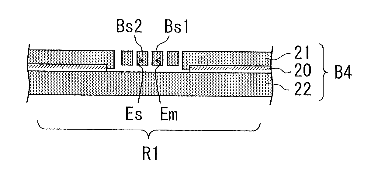
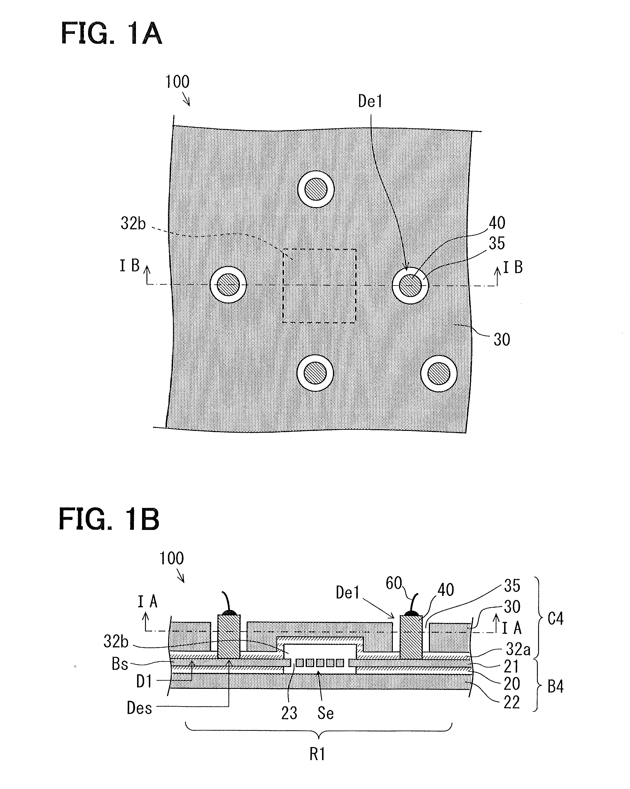
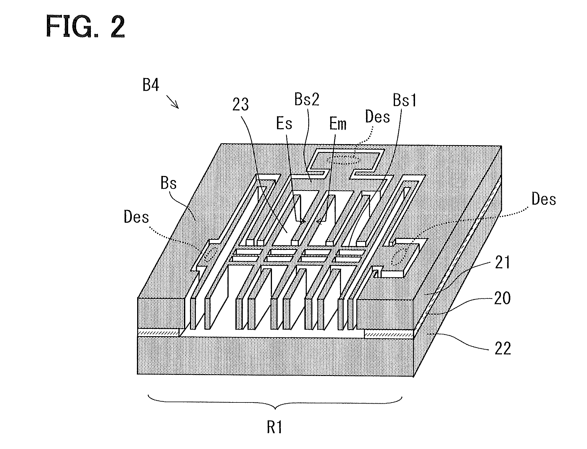
[0071]FIG. 1A is a schematic plan view of a part of a semiconductor device 100 as an example of the semiconductor device according to an embodiment. FIG. 1B is a schematic cross-sectional view taken along a line IB-IB in FIG. 1A. FIG. 1A is also a cross-section taken along a line IA-IA in FIG. 1BFIG. 2 is a perspective view of a base substrate of the semiconductor device 100 shown in FIGS. 1A and 1B.

[0072]In FIGS. 1A, 1B and 2 like parts which correspond to parts of the semiconductor devices 91, 92 of FIGS. 30 and 31, are designated with like reference characters.

[0073]Referring to FIGS. 1A and 1 B, the semiconductor device 100 has a base substrate B4 made of silicon and a cap substrate C4 made of silicon. The base substrate B4 and the cap substrate C4 are bonded to each other at a bonding surface D1.

[0074]The semiconductor device 100 includes a mechanical quantity sensor element using an inertia force. A sensing portion Se for detecting mechanical quantity such as acceleration and ...


PUM


Abstract

A semiconductor device includes a base substrate made of silicon, a cap substrate and a leading electrode having a metal part. The base substrate has base semiconductor regions being insulated and separated from each other at a predetermined portion of a surface layer thereof. The cap substrate is bonded to the predetermined portion of the surface layer of the base substrate. The leading electrode has a first end connected to one of the plurality of base semiconductor regions of the base substrate Wand extends through the cap substrate such that a second end of the leading electrode is located adjacent to a surface of the cap substrate for allowing an electrical connection with an external part, the surface being opposite to a bonding surface at which the base substrate and the cap substrate are bonded. The leading electrode defines a groove between an outer surface thereof and the cap substrate.

Description

CROSS REFERENCE TO RELATED APPLICATION[0001]This application is based on Japanese Patent Applications No. 2009-286874 filed on Dec. 17, 2009 and No. 2010-251092 filed on Nov. 9, 2010, the disclosure of which are incorporated herein by reference.FIELD OF THE INVENTION[0002]The present invention relates to a semiconductor device and a method of manufacturing the same. More particularly, the present invention relates to a semiconductor device having a cap substrate bonded to a base substrate made of silicon for protecting various elements formed in a surface layer of the base substrate, and a method of manufacturing the same.BACKGROUND OF THE INVENTION[0003]In a semiconductor device, it is known to bond a cap substrate to a base substrate for protecting various element formed in a surface layer of the base substrate.[0004]In such a semiconductor device, an electrical connection for electrically connecting the base substrate and an external part is necessary. For example, it is known to...

Claims


Application Information

Patent Timeline
Patent Type & Authority Applications(United States)
IPC IPC(8): H01L23/498H01L21/768
CPCH01L21/768H01L23/498B81B7/007B81B2201/0235B81B2207/095B81C2203/0118H01L21/76898H01L21/84H01L24/03H01L24/05H01L24/48H01L27/1203H01L2224/04042H01L2224/05171H01L2224/05184H01L2224/05556H01L2224/05624H01L2224/05647H01L2224/05669H01L2224/4845H01L2224/48463H01L2924/01004H01L2924/01013H01L2924/01014H01L2924/01029H01L2924/01058H01L2924/01074H01L2924/01078H01L2924/01082H01L2924/014H01L2924/14H01L2924/16235H01L2924/01005H01L2924/01006H01L2924/01024H01L2924/01033H01L2924/01055H01L2924/01072H01L2924/1461H01L2924/00014H01L2924/12036H01L21/7682H01L2924/00H01L2224/45099
Inventor TANAKA, MASAYAFUJII, TETSUO
Owner DENSO CORP
Why Eureka
Try Eureka