Thin-film semiconductor device and method for fabricating thin-film semiconductor device

Active Publication Date: 2014-02-27
JOLED INC
View PDF2 Cites 6 Cited by
  • Summary
  • Abstract
  • Description
  • Claims
  • Application Information

AI Technical Summary

Benefits of technology

The present invention is about a way to make a thin-film semiconductor device that has better off-properties (when it's turned off) and lower on-resistance. This means that the device will have less leakage current and can be more efficient in its performance.

Problems solved by technology

As a result, leakage current occurs, degrading the off-characteristics.

Method used


Image

  • Thin-film semiconductor device and method for fabricating thin-film semiconductor device
  • Thin-film semiconductor device and method for fabricating thin-film semiconductor device
  • Thin-film semiconductor device and method for fabricating thin-film semiconductor device

Examples


embodiment

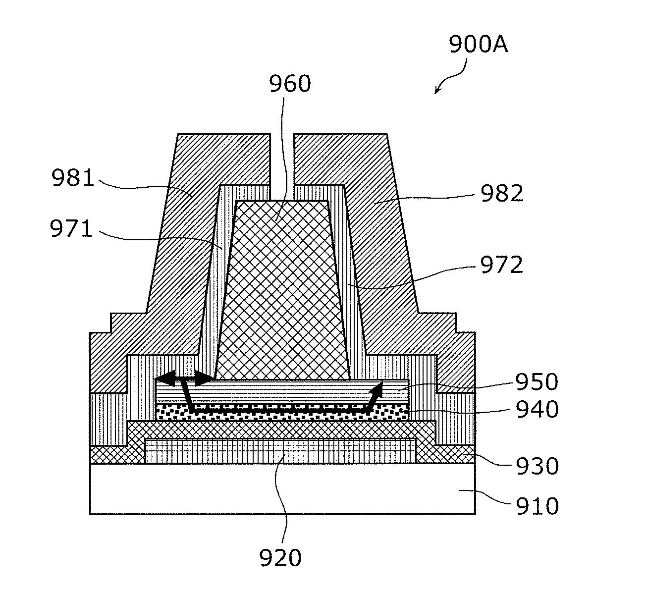
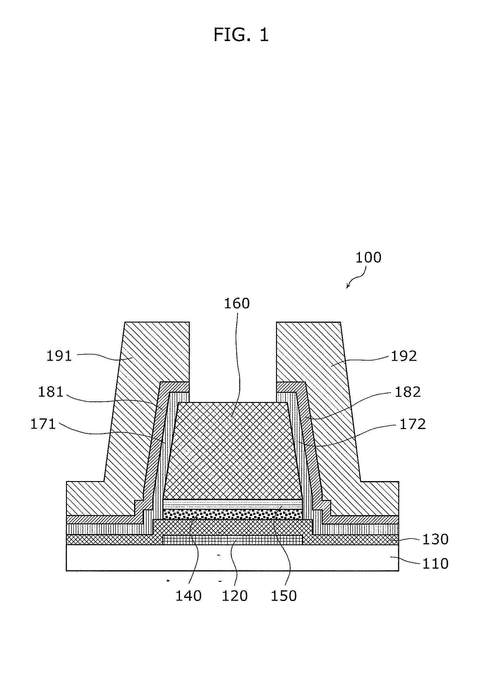
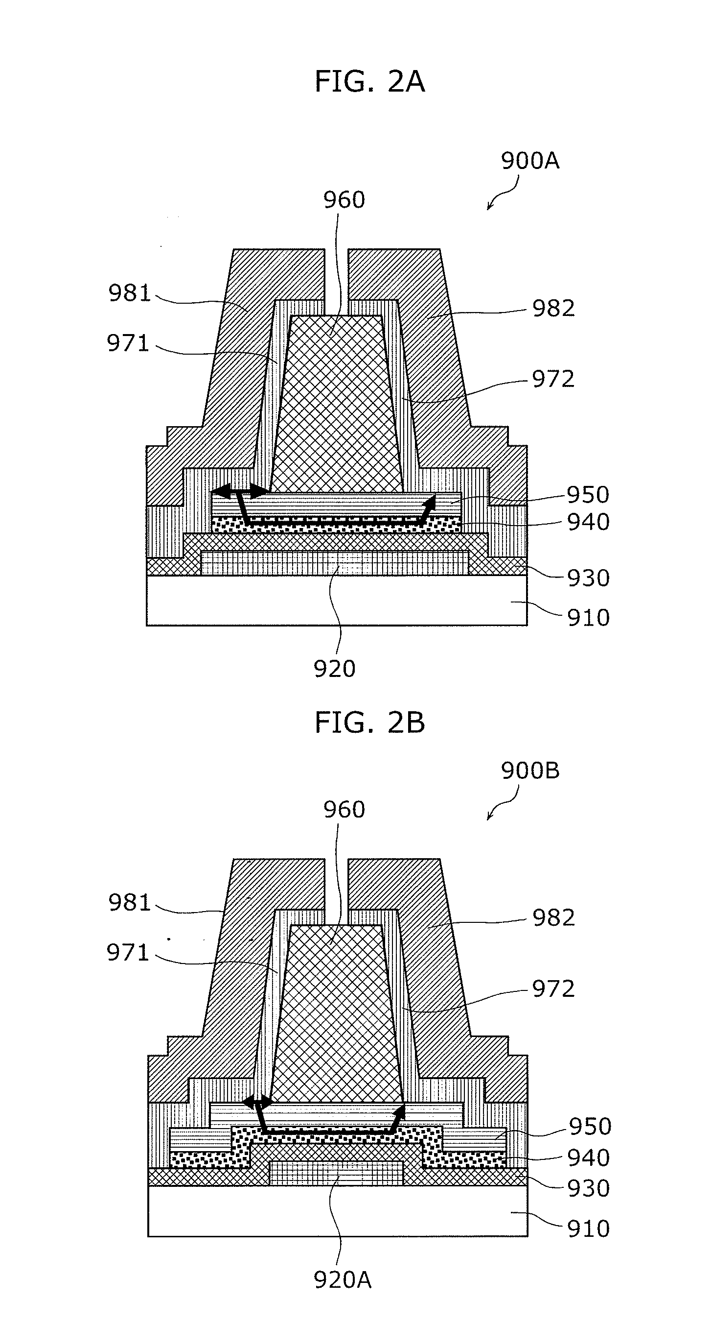
[0047]Hereinafter, descriptions are given of a thin-film semiconductor device and a method for fabricating the thin-film semiconductor device according to the present invention, with reference to the drawings. The embodiment described below shows a preferred specific example of the present invention. Accordingly, the numerical values, shapes, materials, structural elements, the arrangement and connection of the structural elements, steps, the processing order of the steps etc. shown in the following embodiment are mere examples, and therefore do not limit the present invention. Therefore, among the structural elements in the following embodiment, structural elements not recited in any one of claims are not necessarily required to achieve the object of the present invention. Note that, the diagrams are schematic diagrams, and the illustration is not always strictly accurate. Also note that in each diagrams, the same reference numbers indicate elements with the substantially same conf...


PUM


Abstract

A thin-film semiconductor device includes: a gate electrode; a channel layer; a first amorphous semiconductor layer; a channel protective layer; a pair of second amorphous semiconductor layers formed on side surfaces of the channel layer; and a pair of contact layers which contacts the side surfaces of the channel layer via the second amorphous semiconductor layers. The gate electrode, the channel layer, the first amorphous semiconductor layer, and the channel protective layer are stacked so as to have outlines that coincide with one another in a top view. The first amorphous semiconductor layer has a density of localized states higher than those of the second amorphous semiconductor layers. The second amorphous semiconductor layers have band gaps larger than that of the first amorphous semiconductor layer.

Description

TECHNICAL FIELD[0001]The present invention relates to thin-film semiconductor devices, and in particular to a thin-film semiconductor device used for pixel circuits in a display device.BACKGROUND ART[0002]In recent years, organic EL displays using electroluminescence (EL) of an organic material have been attracting attention as a type of next-generation flat panel display replacing liquid crystal displays.[0003]Unlike the voltage-driven liquid crystal display, the organic EL display is a current-driven display device. Accordingly, there is an urgent need for development of a thin-film transistor (TFT) having excellent characteristics as a driving circuit for the active-matrix display device. The TFT is used as a switching device for selecting a pixel or a driving transistor for driving the pixel.[0004]A description is given of a configuration of a conventional thin-film semiconductor device (a thin-film transistor), with reference to FIG. 7 (for example, see Patent Literatures (PLT)...

Claims


Application Information

Patent Timeline
IPC IPC(8): H01L29/786H01L29/66H05B44/00
CPCH01L29/6675H01L29/786H01L29/66765H01L29/78618H01L29/78696H01L21/02532H01L21/0262H01L21/02675H10K59/1213
Inventor KANEGAE, ARINOBUKAWASHIMA, TAKAHIRO
Owner JOLED INC
Why Eureka
Try Eureka