Methods and apparatus for plasma-based deposition

a plasma-based deposition and apparatus technology, applied in chemical vapor deposition coatings, coatings, electric discharge tubes, etc., can solve the problems of high deposition rate in low pressure regimes, achieve high plasma etch selectivity, reduce the overall thermal budget, and achieve high etch selectivity

Active Publication Date: 2014-02-27
NOVELLUS SYSTEMS
View PDF4 Cites 338 Cited by
  • Summary
  • Abstract
  • Description
  • Claims
  • Application Information

AI Technical Summary

Benefits of technology

[0004]High-deposition rate methods for forming transparent ashable hardmasks (AHMs) that have high plasma etch selectivity to underlying layers are provided. The methods involve placing a wafer on a powered electrode such as a powered pedestal for plasma-enhanced deposition. In certain embodiments the pedestal is a dual-frequency powered pedestal. According to various embodiments, the deposition is run at low hydrocarbon precursor partial pressures and/or low process temperatures. Also

Problems solved by technology

In addition, using the powered pedestal results

Method used


Image

  • Methods and apparatus for plasma-based deposition
  • Methods and apparatus for plasma-based deposition
  • Methods and apparatus for plasma-based deposition

Examples


examples

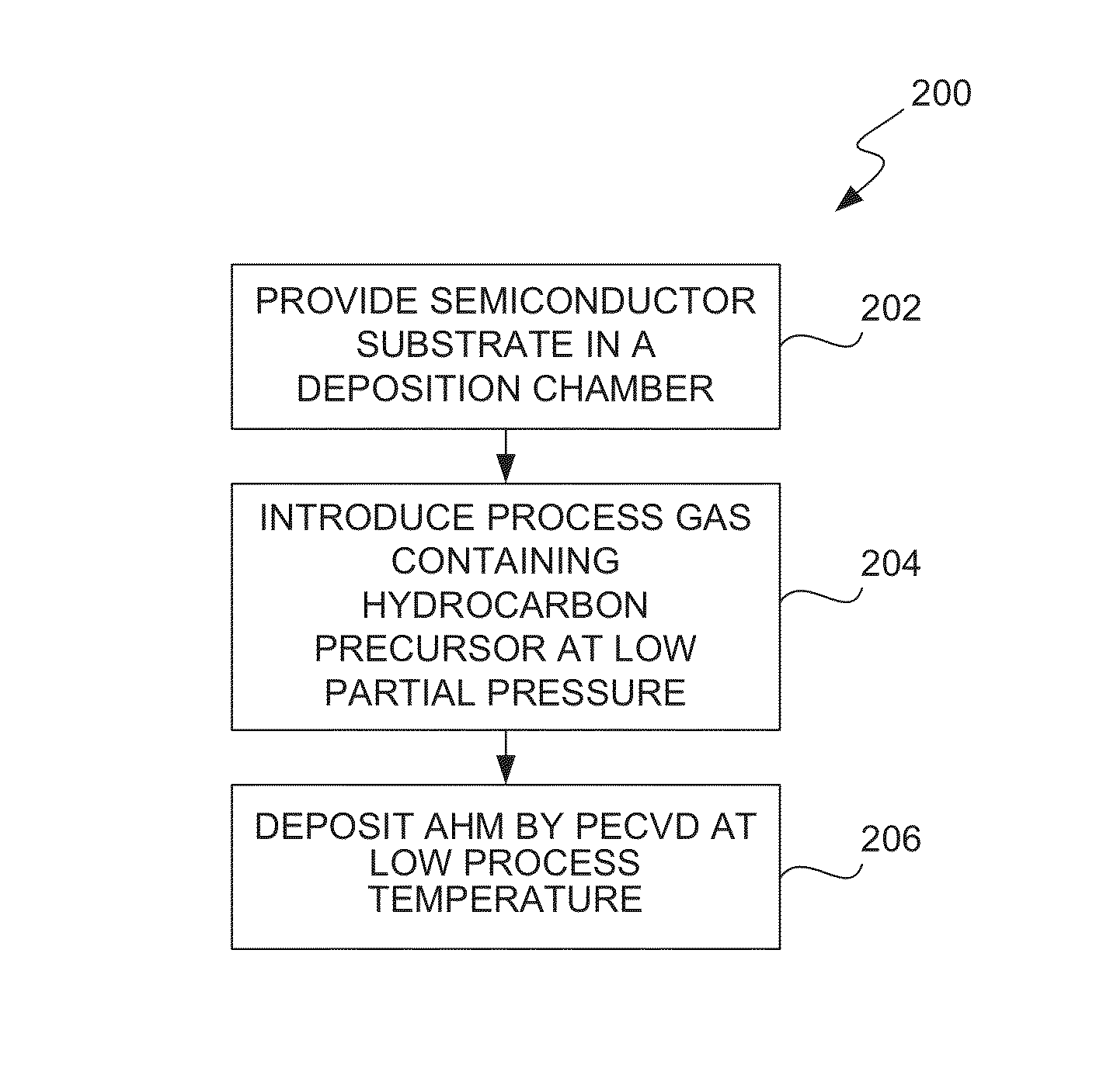
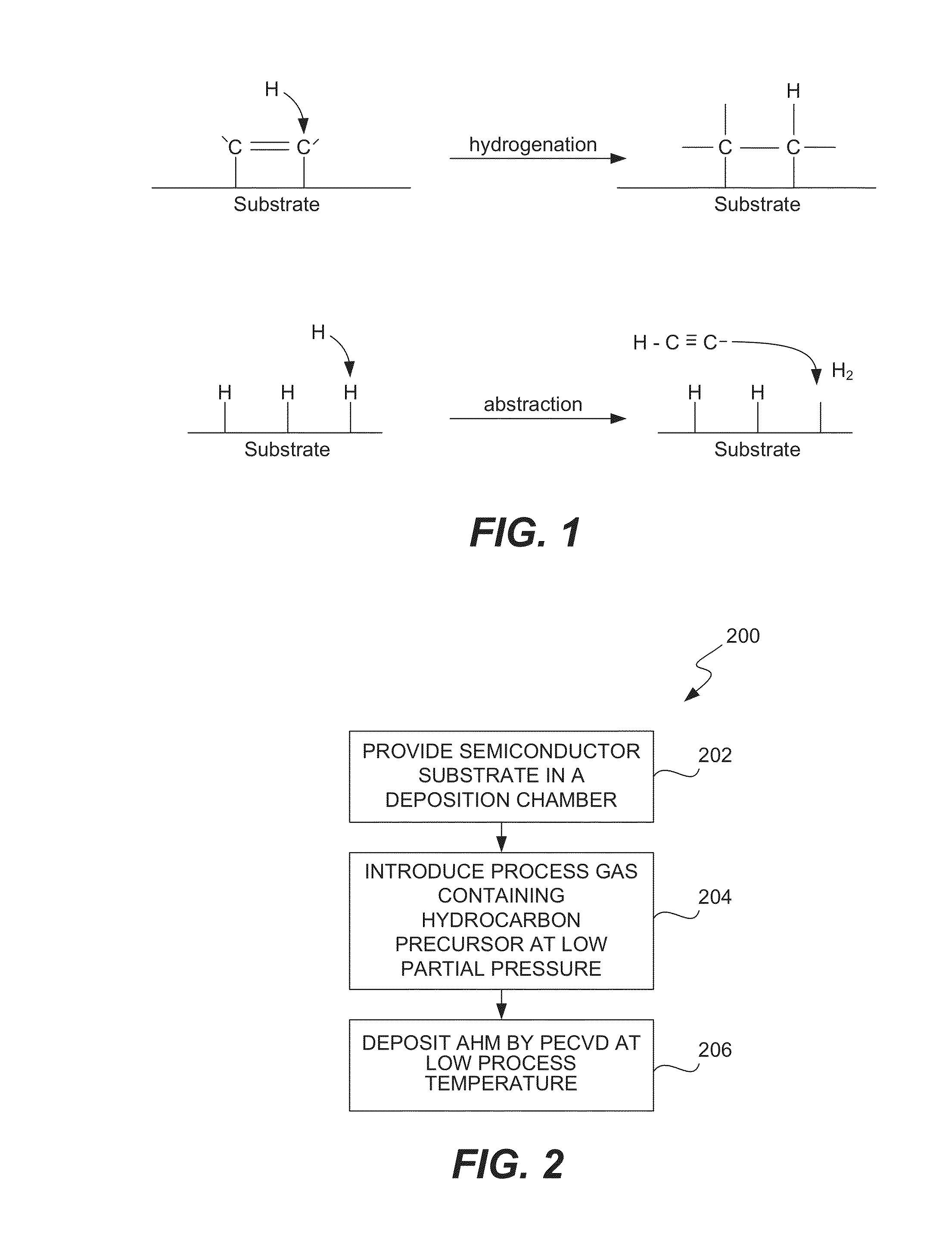
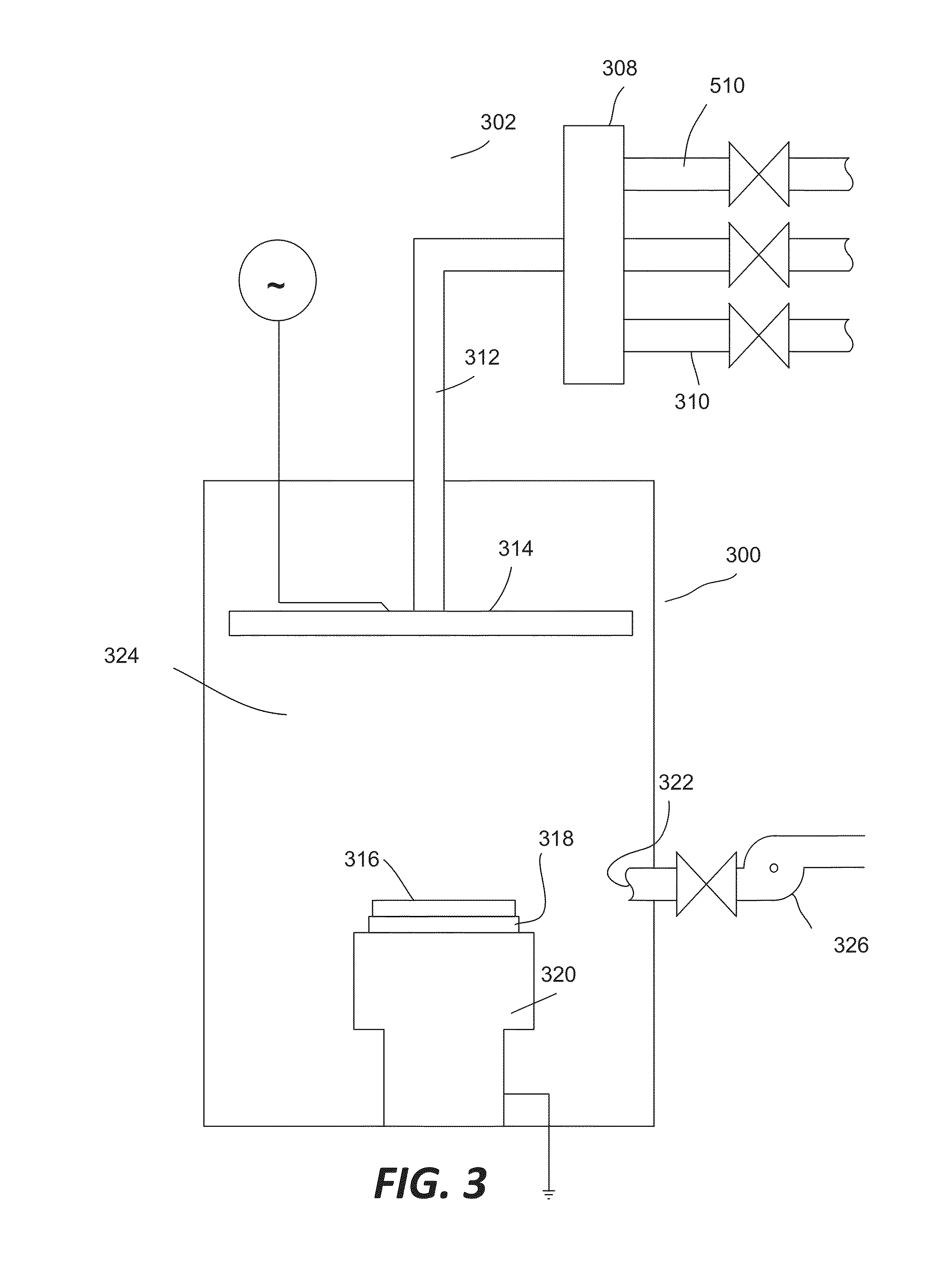
[0058]The following examples are provided to further illustrate aspects and advantages of the present invention. These examples are provided to exemplify and more clearly illustrate aspects of the present invention and are in no way intended to be limiting.

[0059]FIG. 10 shows a rough schematic of a dielectric / AHM / ARL / photoresist film stack. In the stack shown in FIG. 10, a 5000 angstrom AHM overlies a 20,000 angstrom layer of dielectic material (TEOS) on a silicon substrate. A nitrogen free anti-reflective layer (NF ARL) is overlies over the AHM and photoresist overlies the NF ARL. The stack shown in FIG. 10 is just an example of a stack in which an AHM may be employed. In an example application, the portion of the dielectric to be etched is unprotected by the AHM (not shown). The photoresist is patterned and an etch process performed to define the desired features down to the AHM (etch stop) and to etch the unprotected dielectric to define the features in the dielectric. The AHM is...


PUM

PropertyMeasurementUnit
Fractionaaaaaaaaaa
Partial pressureaaaaaaaaaa

Abstract

High-deposition rate methods for forming transparent ashable hardmasks (AHMs) that have high plasma etch selectivity to underlying layers are provided. The methods involve placing a wafer on a powered electrode such as a powered pedestal for plasma-enhanced deposition. According to various embodiments, the deposition is run at low hydrocarbon precursor partial pressures and/or low process temperatures. Also provided are ceramic wafer pedestals with multiple electrode planes embedded with the pedestal are provided. According to various embodiments, the pedestals have multiple RF mesh electrode planes that are connected together such that all the electrode planes are at the same potential.

Description

[0001]This application is a divisional of and claims priority from U.S. patent application Ser. No. 11 / 849,208, filed Aug. 31, 2007, titled “METHODS AND APPARATUS FOR PLASMA-BASED DEPOSITION,” all of which is incorporated herein by this reference for all purposes.BACKGROUND OF THE INVENTION[0002]Ceramic pedestals are useful in applications in which processing temperatures are too high for aluminum pedestals to withstand. One such application is the deposition of ashable hardmasks (AHMs). AHMs are films used in semiconductor processing that may be removed by a technique referred to as “ashing.” In particular, AHMs are often used as etch stop layers. 193 nm or lower lithography schemes require these AHMs to have high etch selectivity to underlying dielectric or metal barrier layers. In addition, 193 nm lithography schemes employ a 633 nm mask alignment laser—requiring the AHM to be transparent to light at 633 nm.[0003]Current methods of producing highly selective AHMs rely on relative...

Claims


Application Information

Patent Timeline
IPC IPC(8): H01L21/469
CPCH01L21/469H01L21/02115H01L21/02271H01L21/31144C23C16/26C23C16/509H01J37/32091
Inventor SUBRAMONIUM, PRAMODBINGHAM, AARONTHOMAS, TIMHENRI, JONFARHNER, GREG
Owner NOVELLUS SYSTEMS
Why Eureka
Try Eureka