Semiconductor unit and semiconductor device using the same

a technology of semiconductor devices and semiconductors, applied in semiconductor devices, semiconductor/solid-state device details, electrical apparatus, etc., can solve the problems of increasing the number of processes and increasing the cost, and achieve the effect of low cos

Active Publication Date: 2014-03-06
FUJI ELECTRIC CO LTD
View PDF1 Cites 19 Cited by
  • Summary
  • Abstract
  • Description
  • Claims
  • Application Information

AI Technical Summary

Benefits of technology

[0016]To address these problems, embodiments of the invention provide a semiconductor unit having chips performing uniform parallel o

Problems solved by technology

For this reason, in the semiconductor module (semiconductor device 500), the number of wires 72

Method used


Image

  • Semiconductor unit and semiconductor device using the same
  • Semiconductor unit and semiconductor device using the same
  • Semiconductor unit and semiconductor device using the same

Examples


example 1

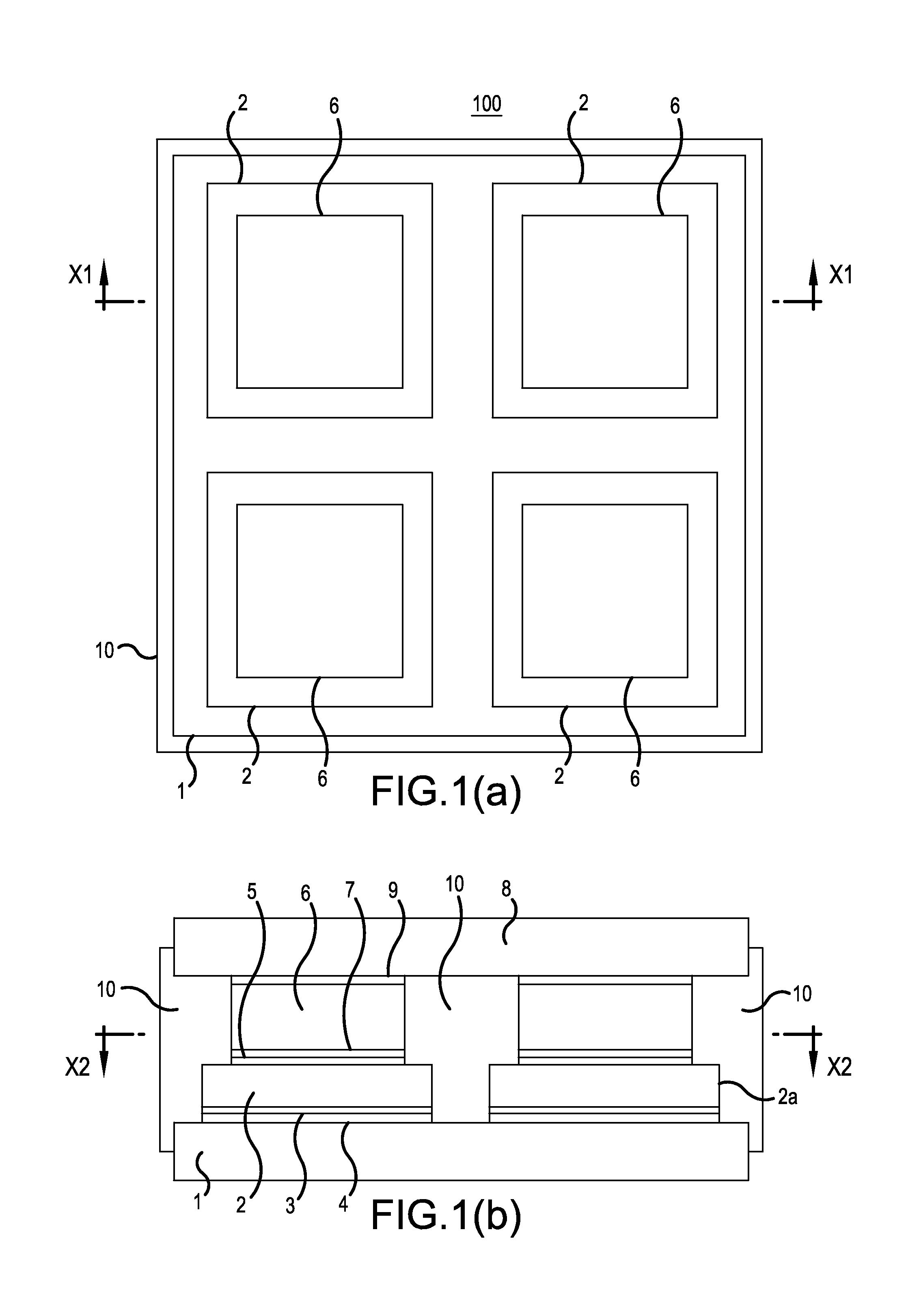
[0032]FIGS. 1(a) and 1(b) are configuration views of a semiconductor unit according to a first example of the invention, in which FIG. 1(a) is a plan view of important part and FIG. 1(b) is a sectional view of important part cut along the line X1-X1 in FIG. 1(a). FIG. 1(a) is a schematic plan view of important part viewed in a direction of the arrow from a plane cut along the line X2-X2 in FIG. 1(b). This semiconductor unit 100 is a semiconductor module having a structure in which a plurality of diode chips (hereinafter referred to as SiC-Di chips) 2 formed on a silicon carbide semiconductor substrate (SiC semiconductor substrate) are connected in parallel.

[0033]Each of the SiC-Di chips 2 is an element in which a cathode electrode 3 is formed on one principal surface while an anode electrode 5 is formed on the other principal surface.

[0034]In this example, cathode electrodes 3 of four SiC-Di chips 2 are joined onto a first common copper plate (first common electrode plate) 1 by sold...

example 2

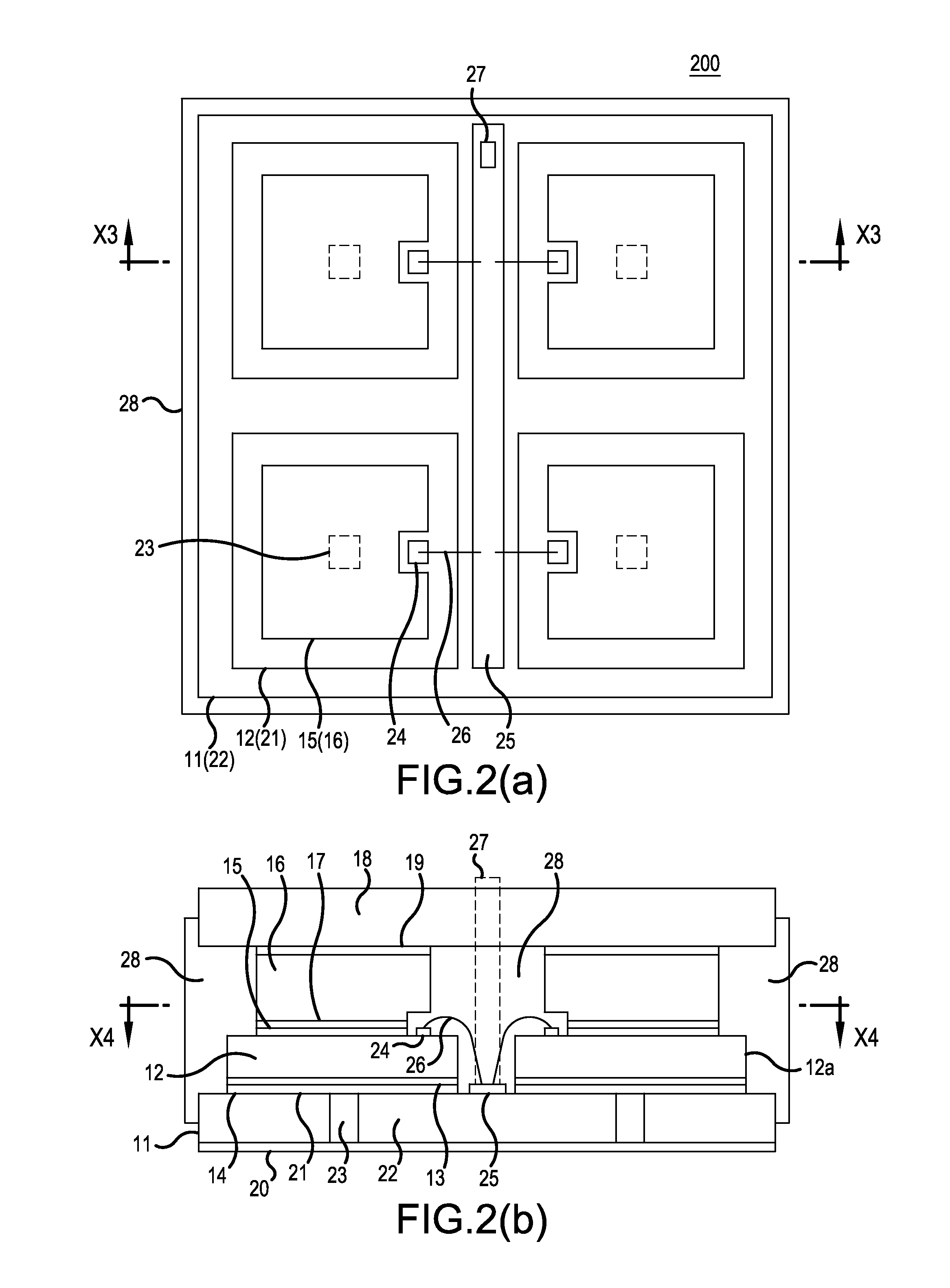
[0039]FIGS. 2(a) and 2(b) are configuration views of a semiconductor unit according to a second example of the invention, in which FIG. 2(a) is a plan view of important part and FIG. 2(b) is a sectional view of important part cut along the line X3-X3 in FIG. 2(a). FIG. 2(a) is a schematic plan view of important part viewed in a direction of the arrow from a plane cut along the line X4-X4 in FIG. 2(b). This semiconductor unit 200 is a semiconductor module having a structure in which a plurality of SiC-MOSFET chips 12 formed on an SiC semiconductor substrate are connected in parallel.

[0040]Here, the SiC-MOSFET chips 12 are an instance of SiC switching devices. SiC-JFETs (Junction Field Effect Transistors), SiC-IGBTs, etc. may be used as the SiC switching devices. The SiC-MOSFET chips 12 will be described below as an instance.

[0041]Each of the SiC-MOSFET chips 12 is an element in which a drain electrode 13 is formed on one principal surface while a source electrode 15 and a gate pad 24...

example 3

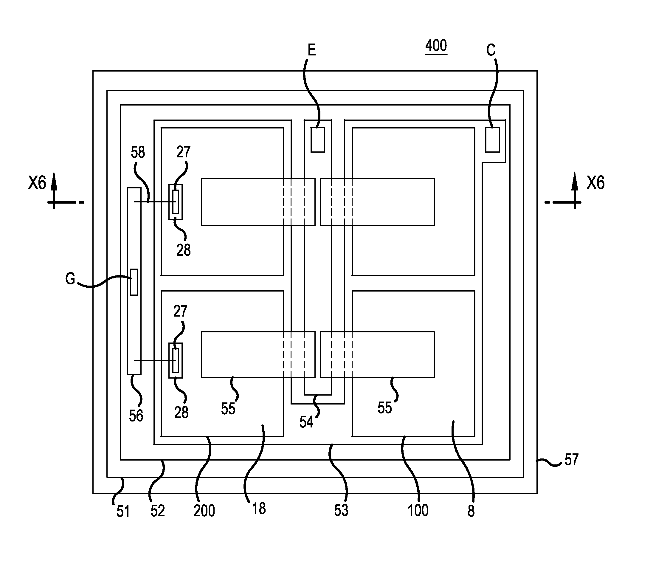
[0053]FIG. 3 are configuration views of a semiconductor device according to a third example of the invention, in which FIG. 3(a) is a plan view of important part and FIG. 3(b) is a sectional view of important part cut along the line X5-X5 in FIG. 3(a). FIG. 3(a) is a schematic arrangement view in a casing 44.

[0054]This semiconductor device 300 is a semiconductor module having a structure in which semiconductor units 100 formed from SiC-Di chips 2 as free wheeling diodes are back-to-back connected to two Si-IGBT chips 35 to thereby form one upper or lower arm in an inverter. The numbers are not limited thereto.

[0055]A rear metal film 33 of a conductive pattern-including insulating substrate 32 is joined onto a copper base plate 31 by solder not shown, and collector electrodes 36 of the two Si-IGBT chips 35 and first common copper plates 1 of the two semiconductor units 100 formed from the SiC-Di chips 2 are joined onto a third conductive pattern 34 by solder not shown.

[0056]Emitter e...


PUM


Abstract

In some aspects of the invention, semiconductor unit can produce chips performing uniform parallel operation and a low-thermal-resistance. Aspects of the invention can include a plurality of small semiconductor chips of one and the same kind formed by use of an SiC substrate, which is a wide gap substrate are sandwiched between two conductive plates. In this manner, there can be provided a high-reliability semiconductor unit in which parallel operation of the semiconductor chips is uniformized so that breakdown caused by current concentration can be prevented.

Description

CROSS-REFERENCE TO RELATED APPLICATIONS[0001]This application is a continuation of International Application No. PCT / JP2012 / 064145, filed on May 31, 2012, which is based on and claims priority to Japanese Patent Application No. JP 2011-134565, filed on Jun. 16, 2011. The disclosure of the Japanese priority application and the PCT application in their entirety, including the drawings, claims, and the specification thereof, are incorporated herein by reference.BACKGROUND[0002]1. Field of the Invention[0003]The present invention relates to a semiconductor unit having a plurality of semiconductor chips sandwiched between upper and lower conductive plates, and a semiconductor device using this semiconductor unit.[0004]2. Related Art[0005]A semiconductor device having a structure using Si-IGBT (Insulated Gate Bipolar Transistor produced by use of an Si semiconductor substrate) and SiC-Di (Diode produced by use of an SiC semiconductor substrate) as FWD (Free Wheeling Diode) has been develo...

Claims


Application Information

Patent Timeline
IPC IPC(8): H01L23/495
CPCH01L23/49575H01L2224/48137H01L2224/48227H01L2224/49175H01L2224/73265H01L2924/10272H01L2224/32225H01L23/24H01L2224/0603H01L2224/45014H01L2224/45124H01L2224/45147H01L2924/10253H01L2924/1203H01L2924/13055H01L2924/13062H01L2924/13091H01L24/06H01L24/32H01L24/45H01L24/48H01L24/49H01L24/73H01L25/072H01L2224/04026H01L2224/04042H01L2224/06181H01L2224/291H01L2224/32245H01L2224/48139H01L2224/73215H01L2924/19107H01L2924/30107H01L23/3735H01L23/4334H01L23/492H01L23/49811H01L2224/49111H01L2924/01047H01L23/053H01L24/33H01L2224/33181H01L2224/4903H01L2924/12041H01L2924/1033H01L25/03H01L2924/1306H01L2924/12032H01L2924/1305H01L2924/12036H01L2924/181H01L2924/00014H01L2224/73221H01L2224/2612H01L2224/49113H01L2924/00012H01L2924/014H01L2924/00H01L2924/206H01L23/48
Inventor MIYANAGI, TOSHIYUKI
Owner FUJI ELECTRIC CO LTD
Why Eureka
Try Eureka