Electric charge detection circuit

a detection circuit and charge technology, applied in the direction of resistance/reactance/impedence, capacitance measurement, instruments, etc., can solve problems such as unresolved problems, suppress dc voltage fluctuations, suppress noise density increases, and suppress drain voltage fluctuations.

Inactive Publication Date: 2014-03-06
FUJI ELECTRIC CO LTD
View PDF0 Cites 6 Cited by
  • Summary
  • Abstract
  • Description
  • Claims
  • Application Information

AI Technical Summary

Benefits of technology

[0024]By way of the low pass filter, embodiments of invention allow suppressing fluctuation of DC voltage of the DC voltage source, and allows suppressing fluctuation of the drain voltage of the field effect transistor.
[0025]In a fifth aspect of the electric charge detection circuit according to embodiments of the present invention, the drain voltage adjustment circuit uses a current mirror circuit as a load of the differential inputs, the drain voltage adjustment circuit that having a cascode-connected voltage control active element that adjusts the drain voltage of the field effect transistor that is connected to a reference current side of the current mirror circuit.
[0026]In a case where a current mirror circuit is used as a load, embodiments of the above configuration allow adjusting the drain voltage of the field effect transistor, by way of a drain voltage adjustment circuit, on the reference current side of the current mirror circuit.
[0027]In a sixth aspect of the electric charge detection circuit according to embodiments of the present invention, the drain voltage adjustment circuit uses a current mirror circuit as a load of the differential inputs, a negative electrode input terminal of a second differential amplifier is connected to the drain of a field effect transistor that is connected to a mirror current side of the current mirror circuit, and the voltage at the positive electrode input terminal of the second differential amplifier is controlled, thereby adjusting the drain voltage of the field effect transistor that is connected to the mirror current side.
[0028]By virtue of the above configuration, the voltage at the positive electrode input terminal is controlled through connection of the DC voltage source to the control side of the second differential amplifier, so that, as a result, the drain potential of the field effect transistor on the mirror current side and the potential of the DC voltage source are equalized, and the input capacitance of the field effect transistor on the mirror current side can be rendered variable by making variable the DC voltage source.
[0029]In the electric charge detection circuit of embodiments of the present invention, thus, the drain voltage of at least one of two field effect transistors that make up a differential amplifier circuit is adjusted by a drain voltage adjustment circuit, in a case where a physical quantity detection sensor that comprises an electric charge generation-type sensor and a capacitance change-type sensor are driven with AC bias; as a result, this elicits the effect of making it possible to suppress increases in noise density through accurate adjustment of the input capacitance of at least one of positive and negative differential inputs.

Problems solved by technology

The source of this noise is the leakage current of the variable-capacitance diodes D1 and D2 that are used as variable-capacitance devices, and which cannot thus be used as they are in an AC bias method of high SN.
This constitutes an unresolved problem.

Method used


Image

  • Electric charge detection circuit
  • Electric charge detection circuit
  • Electric charge detection circuit

Examples


first embodiment

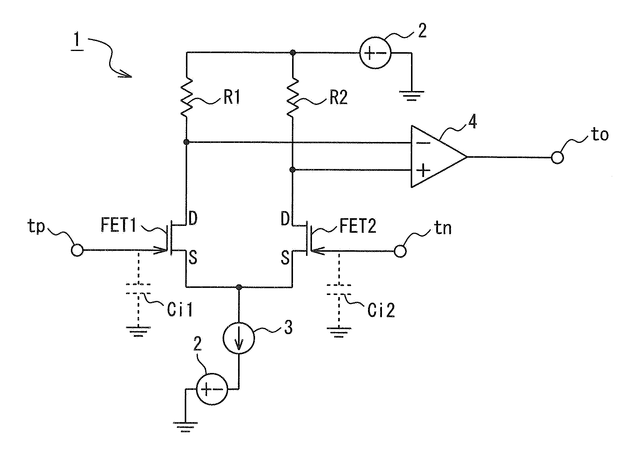
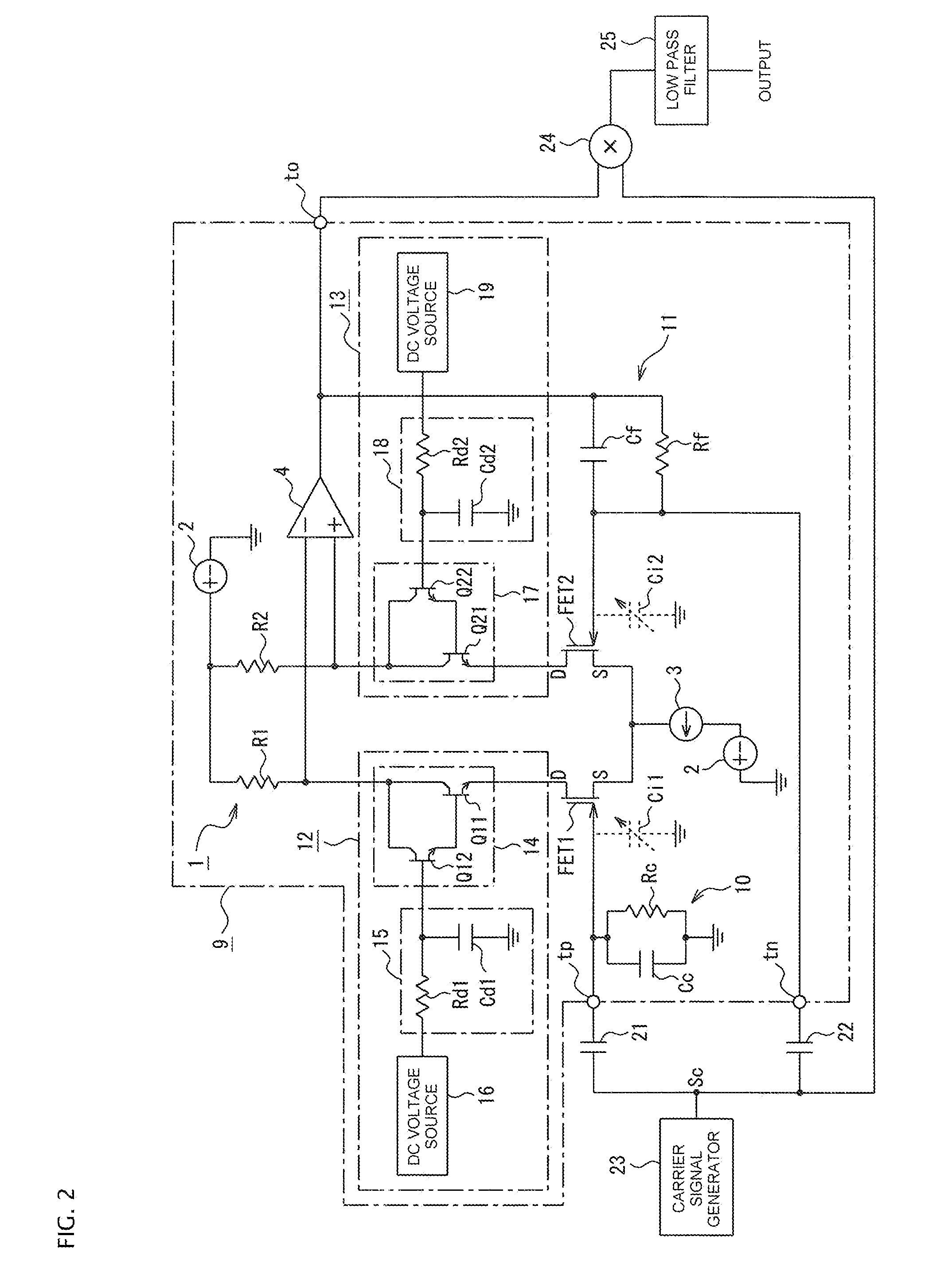
[0052]In the present invention, therefore, an electric charge detection circuit 9 is configured, as illustrated in FIG. 2, with a view to modifying the drain voltages of the field effect transistors FET 1 and FET 2.

[0053]Specifically, the electric charge detection circuit 9 has the above-described differential amplifier circuit 1 illustrated in FIG. 1. A cancel circuit 10 in which a cancel resistor Rc and a cancel capacitor Cc are connected in parallel is connected between ground and a connection point between the gate of the field effect transistor FET 1 and the positive electrode input terminal tp of the differential amplifier circuit 1. A feedback circuit 11 in which a feedback resistor Rf and a feedback capacitor Cf are connected in parallel is connected between the negative electrode input terminal to and the output side of the differential amplifier 4.

[0054]Drain voltage adjustment circuits 12 and 13 that adjust drain voltage are respectively interposed between the field effec...

second embodiment

[0082]the present invention is explained next with reference to FIG. 8.

[0083]In the second embodiment, the load resistors R1 and R2 have been omitted, and the current mirror circuit constitutes a load.

[0084]In the second embodiment, the load resistors R1 and R2 that are the initial stage of the differential amplifier circuit 1 in the configuration of FIG. 2 of the first embodiment described above have been omitted, as illustrated in FIG. 8, and a current mirror circuit 31 is connected, as a load, instead of the load resistors R1 and R2. The current mirror circuit 31 has pnp-type bipolar transistors Q31 and Q32 the emitters whereof are connected to the positive electrode side of the DC voltage source 2, and has a configuration wherein the bases of both bipolar transistors Q31 and Q32 are connected to each other, and the midpoint between bases is connected to the collector of the bipolar transistor Q31.

[0085]A drain voltage adjustment circuit 12 identical to that of the first embodime...

third embodiment

[0088]the present invention is explained next with reference to FIG. 9.

[0089]In the third embodiment there is modified the input capacitance of a field effect transistor on the mirror current side, in a case where a current mirror circuit is used as a load.

[0090]In the third embodiment, specifically, the drain voltage adjustment circuit 12 in the configuration of FIG. 8 described above is omitted; instead, the drain voltage adjustment circuit 13 is provided on the mirror current side of the current mirror circuit 31, as illustrated in FIG. 9.

[0091]The drain voltage adjustment circuit 13 has a configuration wherein the connection point between the bipolar transistor Q32 and the field effect transistor FET 2 is connected to a negative electrode input terminal of a differential amplifier 41 that comprises an operational amplifier, the DC voltage source 19 is connected to the positive electrode input terminal of the differential amplifier 41, and the output side of the differential ampl...


PUM


Abstract

Ends on one side of physical quantity detection sensors formed of any of an electric charge generation-type sensor and a capacitance change-type sensor can be connected to negative electrode input terminals of a differential amplifier circuit, and ends on the other side are connected to positive electrode input terminals of the differential amplifier circuit. A feedback resistor and a feedback capacitor are connected in parallel between the negative electrode input terminal and an output terminal of the differential amplifier circuit, and a cancel resistor and a cancel capacitor are connected in parallel between a reference voltage and the positive electrode input terminal of the differential amplifier circuit. Drain voltage adjustment circuits can be provided that adjust the drain voltage of at least one of two field effect transistors to which positive and negative differential inputs of the differential amplifier circuit are individually inputted.

Description

CROSS-REFERENCE TO RELATED APPLICATIONS[0001]This application is a continuation of International Application No. PCT / JP20111006349, filed on Nov. 14, 2011, which is based on and claims priority to Japanese Patent Application No. JP 2010-180986, filed on Aug. 12, 2010. The disclosure of the Japanese priority application and the PCT application in their entirety, including the drawings, claims, and the specification thereof, are incorporated herein by reference.BACKGROUND OF THE INVENTION[0002]1. Field of the Invention[0003]Embodiments of the present invention relate to electric charge detection circuits that detect electric charge in an electric charge generation-type sensor or capacitance change-type sensor such as a pressure sensor, a microphone, an acceleration sensor, an angular velocity sensor, a strain gauge or the like.[0004]2. Description of the Related Art[0005]Typical examples of electric charge generation-type sensors include, for instance, strain gauges and acceleration s...

Claims


Application Information

Patent Timeline
Patent Type & Authority Applications(United States)
IPC IPC(8): G01R29/24
CPCG01R29/24G01D5/24G01R27/2605
Inventor SUZUKI, TAKESHIMATSUO, NAOYUKIKISHIRO, MASAMI
Owner FUJI ELECTRIC CO LTD
Why Eureka
Try Eureka