Display device and manufacturing method thereof

a technology of display device and manufacturing method, which is applied in the manufacture of electric discharge tubes/lamps, instruments, and final products. it can solve the problems of affecting the reliability of the conventional display device. it can improve the reliability of the transistor, suppress the increase in an area of the periphery, and improve the reliability of the display element.

Active Publication Date: 2014-03-06
SEMICON ENERGY LAB CO LTD
View PDF9 Cites 111 Cited by
  • Summary
  • Abstract
  • Description
  • Claims
  • Application Information

AI Technical Summary

Benefits of technology

[0033]According to one embodiment of the present invention, a method for manufacturing the display device in which reliability of a display element is improved can be provided.
[0034]According to one embodiment of the present invention, a method for manufacturing th...

Problems solved by technology

However, there has been a problem in that the long-term reliability of the conventional display device is not sufficiently secured.
Note that in the case where moisture such as water enters from the outside to the inside of the sealed region, characteristics of the display element and a transistor for d...

Method used


Image

  • Display device and manufacturing method thereof
  • Display device and manufacturing method thereof
  • Display device and manufacturing method thereof

Examples


embodiment 1

[0058]In this embodiment, one embodiment of a display device according to the present invention is described with reference to FIGS. 1A and 1B, FIGS. 2A to 2C, and FIG. 3.

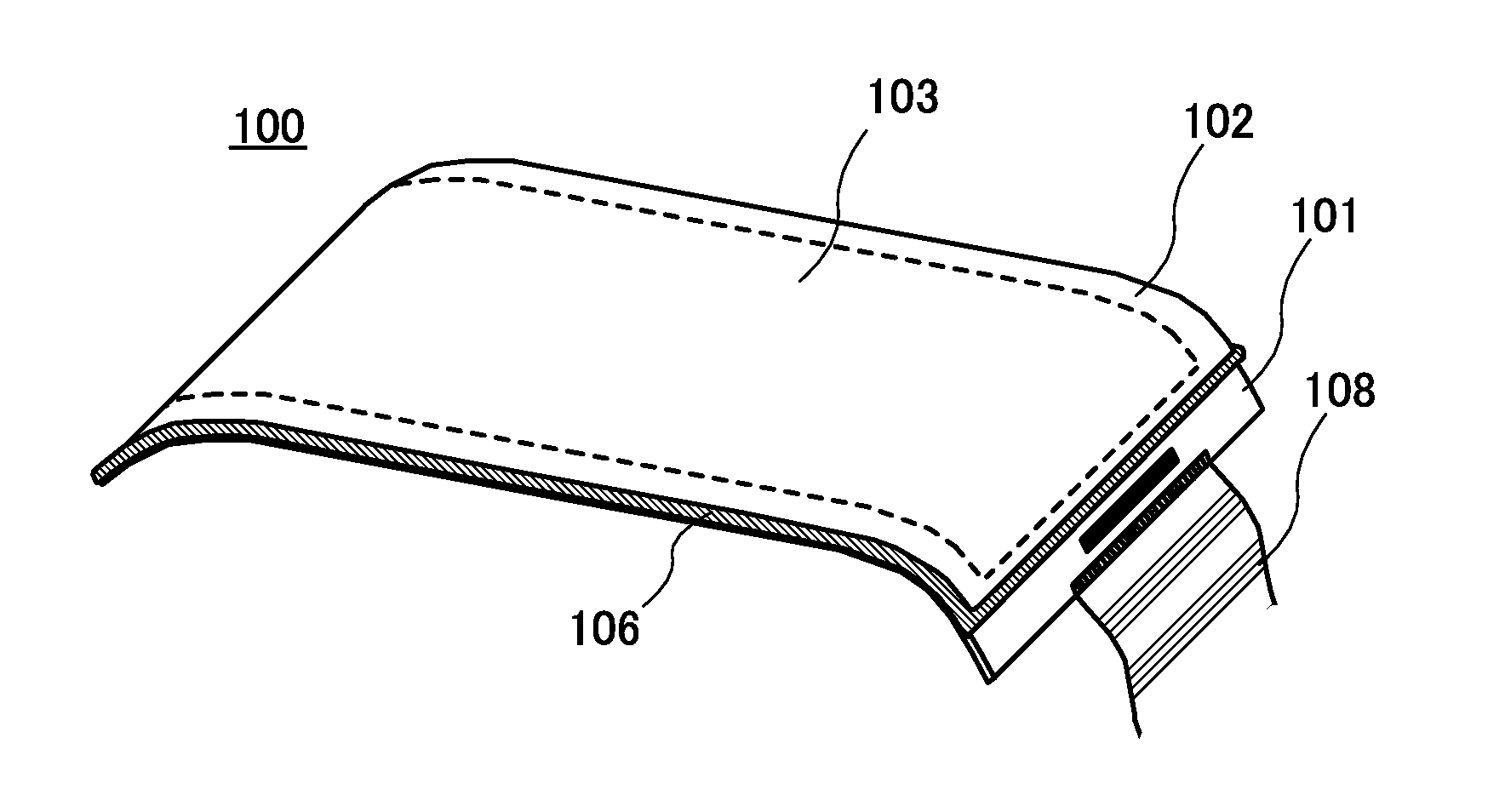
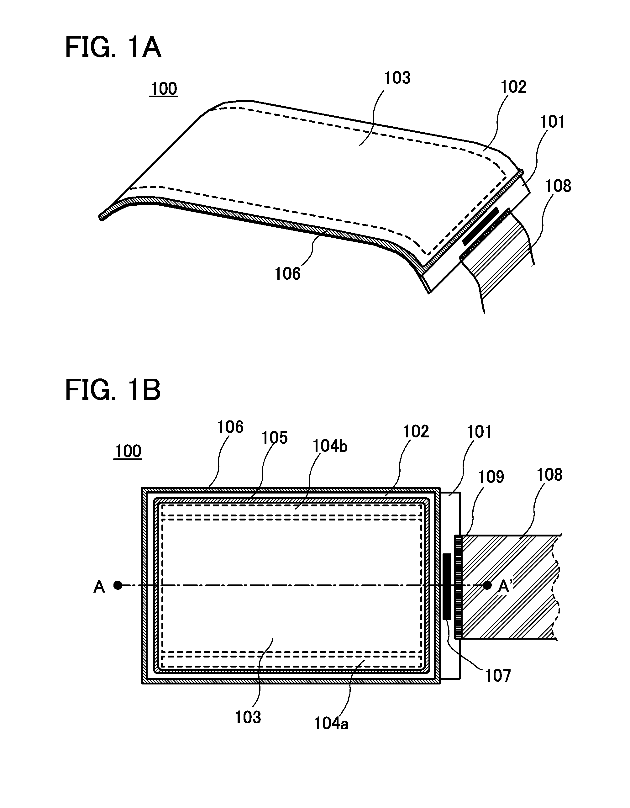
[0059]FIG. 1A is a bird's-eye perspective view of one embodiment of a display device according to the present invention. A display device 100 includes a flexible substrate 101, a flexible substrate 102 which is provided to face the flexible substrate 101, and a flexible printed circuit (FPC) 108 which is electrically connected to the flexible substrate 101. The flexible substrate 101 is bonded to the flexible substrate 102 by a sealant (not illustrated), and a sealant 106, which is different from the above sealant, is further provided on the side surfaces of the flexible substrate 101 and the flexible substrate 102.

[0060]As illustrated in FIG. 1A, the display device according to the present invention uses flexible substrates as a pair of electrodes facing each other. Thus, the whole display device 100 has flexibili...

embodiment 2

[0107]In this embodiment, as an example of a method for manufacturing the display device according to the present invention, a method for manufacturing the display device 100a described in Embodiment 1 is described with reference to FIGS. 4A to 4D and FIGS. 5A to 5C.

[0108]First, as illustrated in FIG. 4A, the element layer 111 is formed over the flexible substrate 101 with the insulating layer 110 provided therebetween.

[0109]As the flexible substrate 101, for example, a flexible metal base can be used. As the base, a thin base (e.g., a sheet or a film) containing a metal element, specifically, a metal sheet or a metal film of titanium or the like, or an alloy sheet or an alloy film of stainless steel or the like can be used. Among them, a sheet or a film of stainless steel which is relatively inexpensive and available is preferable.

[0110]Further, other than the metal base, a resin base having heat resistance may be used. As the resin base, a flexible substrate can be used; for examp...

embodiment 3

[0146]In this embodiment, one embodiment of a display device according to the present invention, which is different from the display device described in Embodiment 1, is described with reference to FIGS. 6A and 6B, FIGS. 7A to 7C, and FIG. 8.

[0147]FIG. 6A is a bird's-eye perspective view of one embodiment of a display device according to the present invention. A display device 200 is different from the display device 100 described in Embodiment 1 in that shapes of a flexible substrate 201 and a flexible substrate 202 are substantially the same and there is no offset region.

[0148]The display device 200 includes the flexible substrate 201, the flexible substrate 202 which is provided to face the flexible substrate 201, and an FPC (flexible printed circuit) 208 which is electrically connected to the flexible substrate 201. The flexible substrate 201 is electrically connected to the FPC 208 through an opening formed in the flexible substrate 202, which is described later. The flexible s...


PUM


Abstract

A display device in which reliability of a display element is improved is provided. Alternatively, a display device in which reliability of a transistor is improved is provided. Alternatively, a display device in which an increase in an area of a periphery region is suppressed is provided. A display device includes a display region including a display element between a first flexible substrate and a second flexible substrate in which the display region is surrounded by a first continuous sealant, the first sealant is surrounded by a second continuous sealant, and the second sealant is provided between the first substrate and the second substrate and on at least one of a side surface of the first substrate and a side surface of the second substrate.

Description

BACKGROUND OF THE INVENTION[0001]1. Field of the Invention[0002]The present invention relates to an object, a method, or a manufacturing method. The present invention relates to a semiconductor device, a display device, a light-emitting device, or a manufacturing method thereof, for example. In particular, the present invention relates to a semiconductor device including an oxide semiconductor, a display device including an oxide semiconductor, or a light-emitting device including an oxide semiconductor, for example. Alternatively, the present invention relates to a display device for displaying an image.[0003]2. Description of the Related Art[0004]A variety of portable electronic devices, such as a cell phone, a smartphone, a personal computer, a tablet terminal, a portable game machine, and a portable music player, have recently come into widespread use.[0005]In the display portion, a light-emitting device including a light-emitting element, a liquid crystal display device, an ele...

Claims


Application Information

Patent Timeline
IPC IPC(8): H01L27/12
CPCH01L27/1214H01L27/1225G02F1/133308G02F1/1339Y02E10/549Y02P70/50H05B33/10H05B33/04H10K50/8426H10K50/841H10K50/844H10K59/1213H10K71/00H10K77/111H10K59/1201H10K2102/311H01L29/7869
Inventor YAMAZAKI, SHUNPEIHIRAKATA, YOSHIHARUNISHI, TAKESHI
Owner SEMICON ENERGY LAB CO LTD
Why Eureka
Try Eureka