Synaptic semiconductor device and operation method thereof

a semiconductor and synaptic technology, applied in the field of synaptic semiconductor devices and operation methods thereof, can solve the problems of inability to mimic short-term memory, and inability to embodie short-term memory transitions

Active Publication Date: 2014-03-06
SEOUL NAT UNIV R&DB FOUND
View PDF1 Cites 20 Cited by
  • Summary
  • Abstract
  • Description
  • Claims
  • Application Information

AI Technical Summary

Benefits of technology

[0047]In short, the present invention provides a low power synaptic semiconductor device that can mimic not only the short-term memory in a nervous system of a living body, but also the short- and long-term memory transition property and the causal inference property of a living body due to the time difference of signals of the pre- and post-synaptic neurons and be used as a core device to embody a neuromorphic computation system.

Problems solved by technology

But, these cannot mimic the short-term memory that the stored information is naturally deleted within a short time period when the input signal temporarily disappears.
Subsequently, these have a problem that the short-long term memory transition cannot be embodied.
Subsequently, it also has a problem that the short-and long-term memory transition cannot be embodied.

Method used


Image

  • Synaptic semiconductor device and operation method thereof
  • Synaptic semiconductor device and operation method thereof
  • Synaptic semiconductor device and operation method thereof

Examples


Embodiment Construction

[0064]Detailed descriptions of preferred embodiments of the present invention are provided below with respect to accompanying drawings. The structures or the electrical characteristic diagrams of exemplified devices in the accompanying drawings are provided to explain the technical idea of the present invention in order to understand a person with ordinary skill in the art to which the present invention pertains, thus, the technical idea of the present invention should not be restricted to the described embodiments herein.

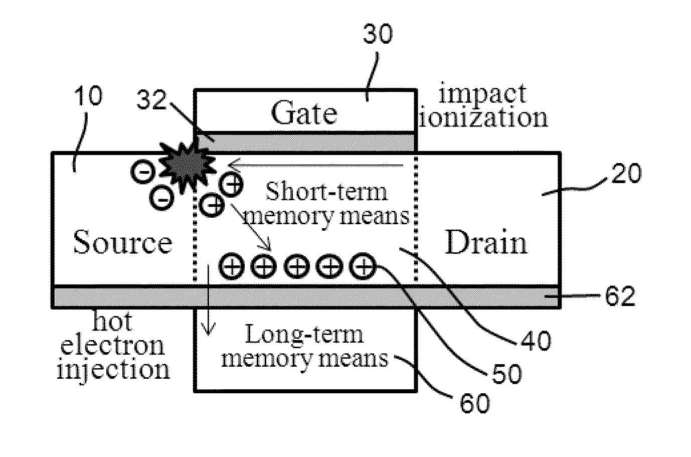
[0065]A synaptic semiconductor device according to an embodiment of the present invention, as shown in FIG. 5, basically comprises: a floating body 40 as a short-term memory means formed of a first conductivity type (e.g., p-type) semiconductor material and electrically isolated from the surroundings; a source 10 and a drain 20 formed of a second conductivity type (e.g., n-type) semiconductor material opposite to the first conductivity type on both sides of the flo...


PUM


Abstract

Disclosed is a semiconductor device used to embody a neuromorphic computation system and operation method thereof. By comprising a floating body as a short-term memory means electrically isolated from the surroundings and a long-term memory means formed at one side of the floating body not formed of a source, a drain and a gate, a low power synaptic semiconductor device is provided, which can be mimic not only the short-term memory in a nervous system of a living body by an impact ionization, but also the short- and long-term memory transition property and the causal inference property of a living body due to the time difference of signals of the pre- and post-synaptic neurons.

Description

CROSS-REFERENCE TO RELATED APPLICATION[0001]This application claims priority to Korean Patent Application No. 10-2012-0098767, filed on Sep. 6, 2012, under 35 U.S.C. 119, the entire contents of which are hereby incorporated by reference.BACKGROUND OF INVENTION[0002]1. Field of the Invention[0003]The present invention relates to a semiconductor device and operation method thereof, and more particularly to a synaptic semiconductor device and operation method thereof.[0004]2. Description of the Related Art[0005]The nervous system of a living body is consisted of numerous nerve cell neurons and synapses connecting neurons. Synapses may be classified as electrical or chemical, based on the signal transmission between neurons. The electrical synapses are found in invertebrates and myocardial cells etc. Since the others are known as the chemical synapses, hereinafter, word of “synapse(s)” indicates the chemical synapse(s).[0006]Recently, many studies have been made to mimic the nervous sys...

Claims


Application Information

Patent Timeline
Patent Type & Authority Applications(United States)
IPC IPC(8): G06N3/02
CPCG06N3/02G06N3/049G06N3/063G11C11/54H01L29/66825
Inventor PARK, BYUNG-GOOKKIM, HYUNGJINKIM, GARAMLEE, JUNG HANKWON, MIN-WOO
Owner SEOUL NAT UNIV R&DB FOUND
Why Eureka
Try Eureka