

Analog-to-digital conversion circuit and method of driving the same
a conversion circuit and analog-to-digital technology, applied in the direction of code conversion, electrical equipment, delta modulation, etc., can solve the problems of limiting the accuracy of the whole system and the improvement of accuracy, so as to suppress an increase in power consumption and improve accuracy.
- Summary
- Abstract
- Description
- Claims
- Application Information
AI Technical Summary
Benefits of technology
Problems solved by technology
Method used
Image

Examples
embodiment 1
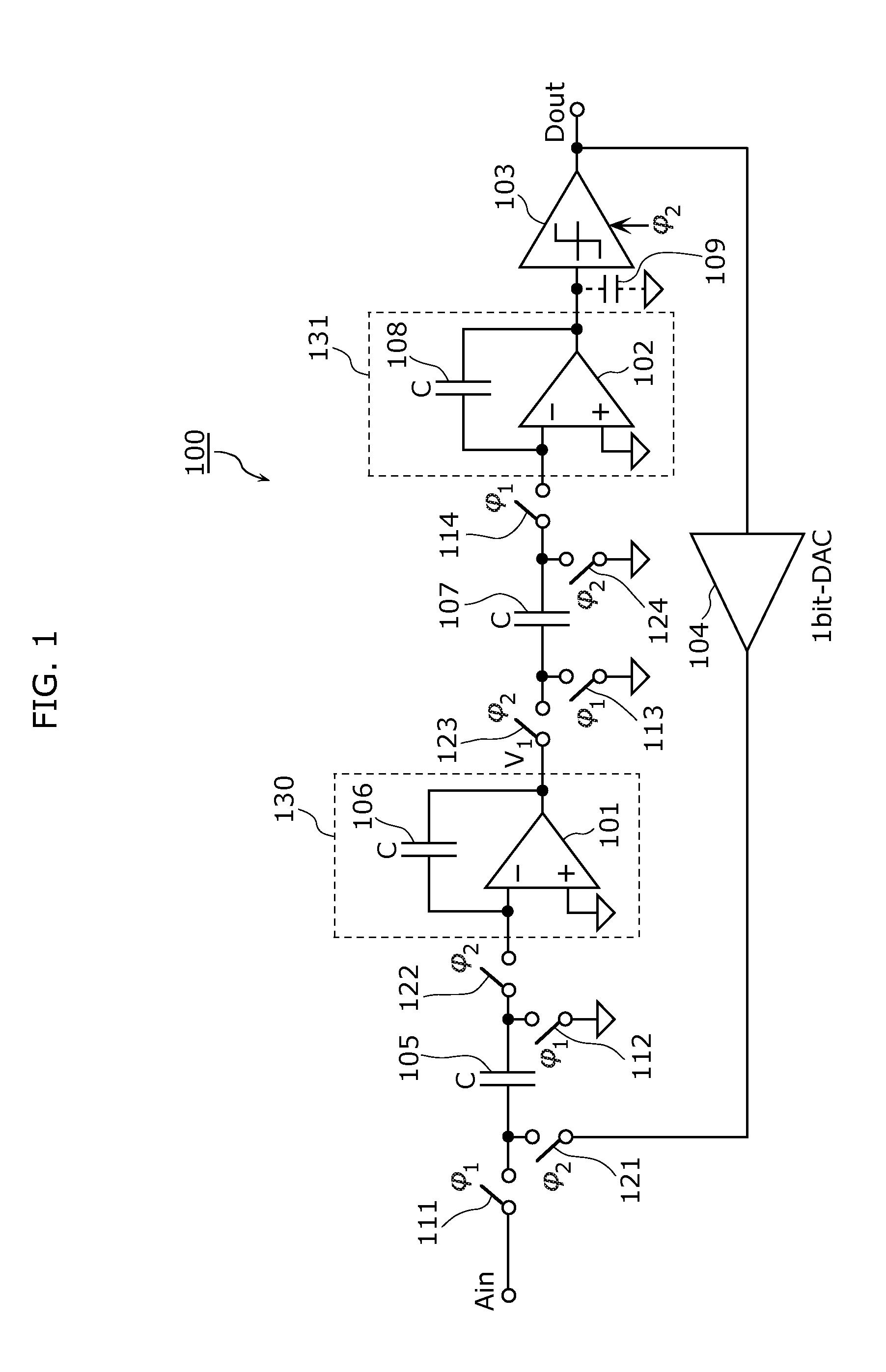
[0061]In an AD conversion circuit according to Embodiment 1 of the present invention, the initial operating period after the reset release (high period or low period) is increased. With this, the AD conversion circuit is capable of improving accuracy by reducing an error between the expected waveform and the actual waveform after the reset release while suppressing an increase in power consumption.
[0062]FIG. 3 is a diagram showing a configuration of the AD conversion circuit according to Embodiment 1 of the present invention. The AD conversion circuit 10 shown in FIG. 3 converts an analog input signal Ain into a digital output signal Dout. The AD conversion circuit 10 includes an AD converter 100 and a clock generating circuit 150.
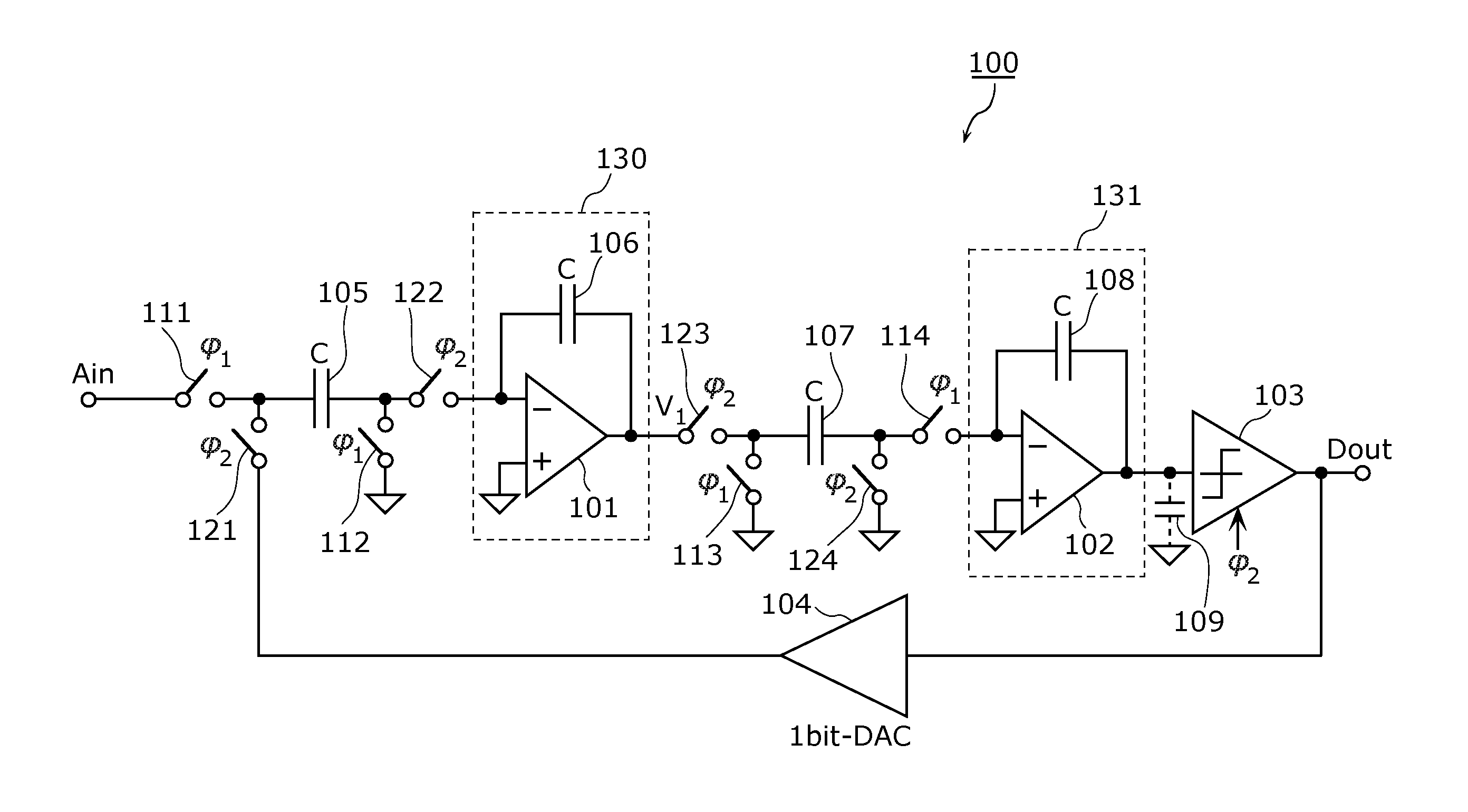
[0063]The AD converter 100 is, for example, a 2nd-order ΔΣ AD converter shown in FIG. 1, and operates using and in synchronization with a clock signal 211 (φ1) and a clock signal 212 (φ2).
[0064]The AD converter 100 shown in FIG. 1 includes integrators 130 ...
embodiment 2
[0096]In this embodiment, a feedforward 2nd-order ΔΣ AD converter according to the present invention is described. It is to be noted that the following mainly describes differences from Embodiment 1 and overlapped descriptions are omitted.
[0097]The overall configuration of the AD conversion circuit according to this embodiment is the same as the configuration shown in FIG. 3 except that the AD converter 100 is replaced with the feedforward 2nd-order ΔΣ AD converter 300.
[0098]FIG. 12 is a circuit diagram showing the feedforward 2nd-order ΔΣ AD converter 300. The AD converter 300 further includes a capacitance adder 330 in addition to the configuration of the AD converter 100 shown in FIG. 1.
[0099]The capacitance adder 330 generates a sum of an analog input signal Ain, an integrated value generated in the integrator 130, and an integrated value generated in the integrator 131. Moreover, the comparator 103 generates a digital output signal Dout by comparing the sum generated by the cap...
embodiment 3
[0112]In this embodiment, an apparatus including the AD conversion circuit 10 described in the above Embodiment 1 or 2 is described.
[0113]First, an image-capturing element 600 including the above AD conversion circuit 10 is described. FIG. 19 is a block diagram showing the image-capturing element 600 according to this embodiment. The image-capturing element 600 includes AD converter arrays 601 and 602, a light-receiving element array 603 in which plural light-receiving elements are arranged in a matrix, a controller 604, and a peripheral circuit 605.
[0114]In general, the number of pixels of the image-capturing element included in a CMOS imaging sensor is determined according to the sensitivity of the light-receiving element, but power consumption of the AD converter is also an important factor. In the case of a general column-parallel AD converter, the AD converter arrays 601 and 602 are positioned above and below the light-receiving element array 603. Moreover, several thousands of...
PUM
 Abstract
Description
Claims
Application Information