Wafer-level RF transmission and radiation devices

a radiation device and transmission line technology, applied in the field of radiation devices, can solve the problems of inability to meet the needs of additional matching networks, thin film designs with a relatively poor impedance match to transceiver circuitry, and known limitations of existing high frequency antennas (e.g. 10 ghz to 300 ghz)

Active Publication Date: 2014-04-17
HARRIS CORP
View PDF2 Cites 7 Cited by
  • Summary
  • Abstract
  • Description
  • Claims
  • Application Information

AI Technical Summary

Benefits of technology

[0009]The invention also concerns a method for constructing a dipole radio frequency antenna. The method includes depositing on a surface of a dielectric substrate a plurality of layers including at least one layer each of a conductive material, a dielectric material, and a sacrificial material. A deposit of the at least one layer of conductive material is controlled to form a transmission line, antenna radiating element and associated antenna feed. The transmission line includes a shield formed of one or more walls and a center conductor disposed coaxially within the shield. The transmission line extends along a surface of the dielectric substrate. A feed port is provided on the transmission line and is comprised of an opening formed on a first wall of the transmission line opposed from the substrate. An antenna feed portion is electrically connected to the cen

Problems solved by technology

However, existing antennas for high frequencies (e.g. 10 GHz to 300 GHz) are known to suffer from certain limitations.
Such designs tend to have relatively low power handling capability.
Moreover, thin film designs with a relatively poor impedance match to transceiver circuitry may re

Method used


Image

  • Wafer-level RF transmission and radiation devices
  • Wafer-level RF transmission and radiation devices
  • Wafer-level RF transmission and radiation devices

Examples


Embodiment Construction

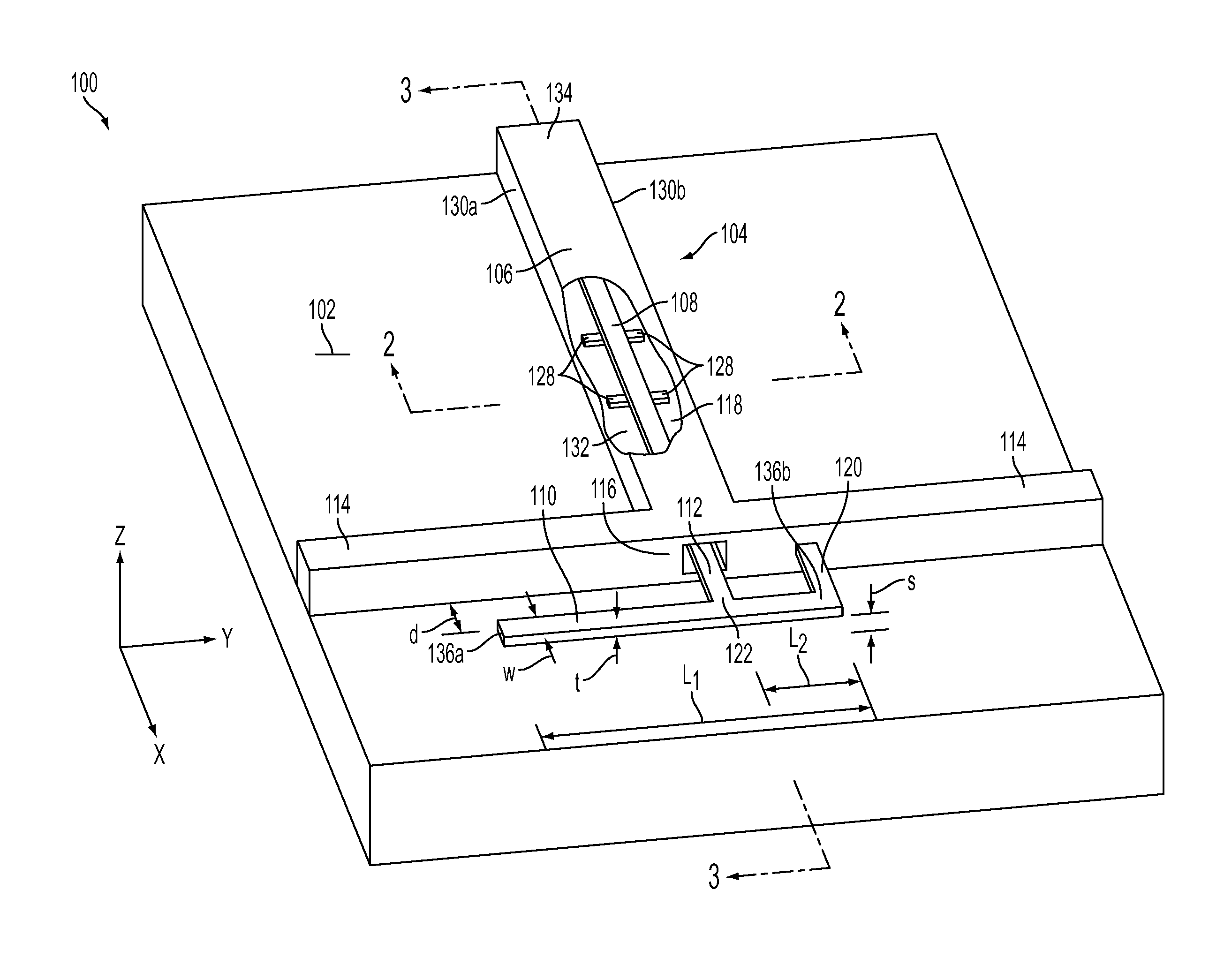
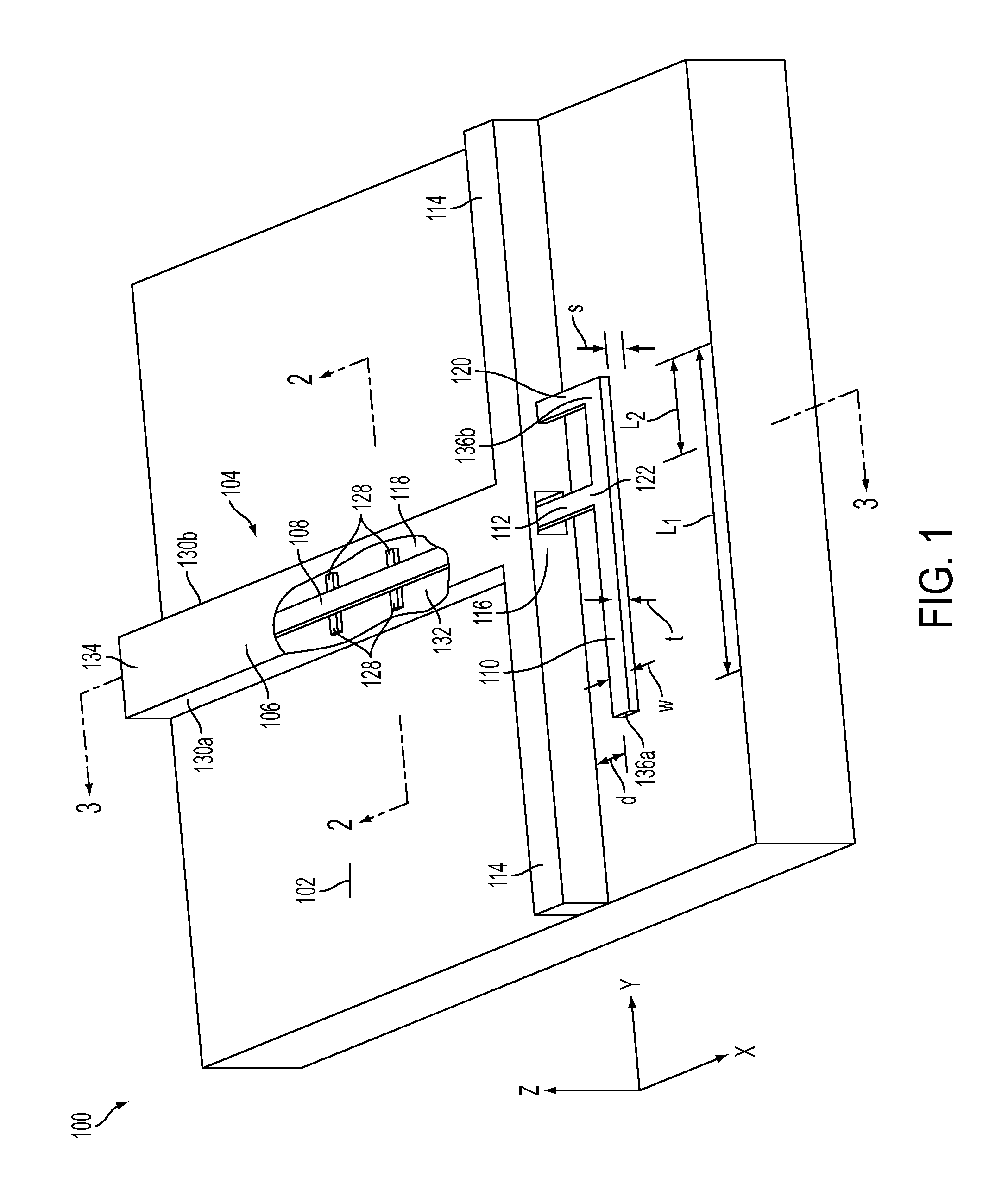
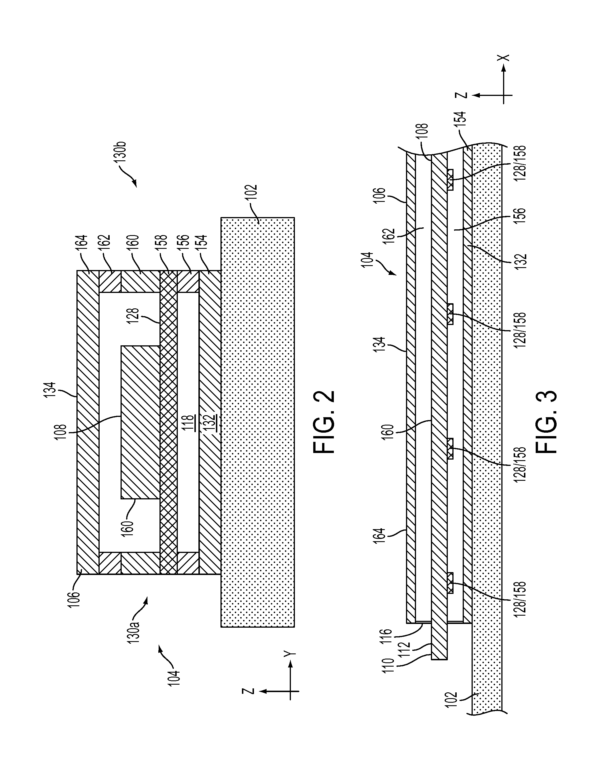
[0019]The invention is described with reference to the attached figures. The figures are not drawn to scale and they are provided merely to illustrate the instant invention. Several aspects of the invention are described below with reference to example applications for illustration. It should be understood that numerous specific details, relationships, and methods are set forth to provide a full understanding of the invention. One having ordinary skill in the relevant art, however, will readily recognize that the invention can be practiced without one or more of the specific details or with other methods. In other instances, well-known structures or operation are not shown in detail to avoid obscuring the invention. The invention is not limited by the illustrated ordering of acts or events, as some acts may occur in different orders and / or concurrently with other acts or events. Furthermore, not all illustrated acts or events are required to implement a methodology in accordance wit...


PUM


Abstract

Method for constructing a dipole radio frequency antenna includes depositing on a dielectric substrate at least one layer each of a conductive material, a dielectric material, and a sacrificial material. The deposit of conductive material is controlled to form a transmission line, antenna radiating element and associated antenna feed. The transmission line includes a shield formed of one or more walls and a center conductor disposed coaxially within the shield. An antenna feed portion is electrically connected to the center conductor and extends through a feed port on the transmission line to connect with an antenna radiating element. The radiating element has an elongated form which extends a first predetermined length transverse to an axis of the transmission line. The method also includes dissolving at least one layer of the sacrificial material to form a clearance space between the surface of the dielectric substrate and the antenna radiating element.

Description

BACKGROUND OF THE INVENTION[0001]1. Statement of the Technical Field[0002]The inventive arrangements relate to wafer level RF devices and more particularly to radiation devices for microwave and millimeter wave communications.[0003]2. Description of the Related Art[0004]Many communication systems operate in high frequency bands. For example, communication systems operating at frequencies as high as 300 GHz are known. Radiation devices, namely antennas, are a necessary element in many such communications system for receiving and transmitting electromagnetic radiation. However, existing antennas for high frequencies (e.g. 10 GHz to 300 GHz) are known to suffer from certain limitations. For example conventional antennas designed for such frequencies are often based on thin film technology. Such designs tend to have relatively low power handling capability. Moreover, thin film designs with a relatively poor impedance match to transceiver circuitry may require additional matching network...

Claims


Application Information

Patent Timeline
IPC IPC(8): H01Q1/38B05D5/12
CPCH01P3/06H01P3/084H01Q9/16H01Q9/42H01Q21/0081
Inventor ROGERS, JOHN E.JACKSON, JR., RONALD E.
Owner HARRIS CORP
Why Eureka
Try Eureka