On-chip HV and LV capacitors acting as the second back-up supplies for nvsram auto-store operation

a technology of nvsram and auto-store operation, which is applied in the direction of static storage, digital storage, instruments, etc., can solve the problems of failure, all on-going read, program and erase operations will be interrupted, and the single memory technology is not acceptable for many medical applications, etc., to achieve the effect of increasing the capacitance of the mim layer for vppcap and vcccap and speeding up the pa

Inactive Publication Date: 2014-04-17
APLUS FLASH TECH
View PDF0 Cites 12 Cited by
  • Summary
  • Abstract
  • Description
  • Claims
  • Application Information

AI Technical Summary

Benefits of technology

[0048]In yet another alternative embodiment, the present invention provides a method for stopping the oscillator and pump circuit when VCC power is removed and the Auto-Store operation of NVSRAM is initiated.
[0049]In still another alternative embodiment, the present invention provides a method for lowering the pump oscillator frequency below 1 / 10 or more during normal SRAM operation to refresh the VPPcap and VCCcap at low current of less than 10 μA.
[0050]In yet still another alternative embodiment, the present invention provides a method for increasing the oscillator frequency to around 2.0 Mhz during normal Software-Store and Hardware-Store operations so that the flash program operation can be done in a faster pace, within 5 ms.
[0051]In one more alternative embodiment, the present invention discloses that the capacitance of the MIM layers for VPPcap and VCCcap can be increased by adding more MIM layers with a metal layer inserted in between as a shielding layer to prevent a coupling effect on normal NVSRAM circuits from VPPcap and VCCcap being discharged.

Problems solved by technology

However, compared with other non-volatile technologies, EEPROM density is lower with a slower Read speed of 100 ns and Write speed of 2 ms, making it unacceptable as a single memory technology for many medical applications.
As a result, both NAND and EEPROM result in limited read / write cycles that can wear out the memory devices in repetitive applications, ultimately causing loss of data.
In the event that VCC in pin1 is removed, all on-going Read, Program and Erase operations will be interrupted and fail because there is no second source of VCC that can immediately replace VCC in pin1 to complete the operation.
Although EEPROM is a non-volatile memory, the new data during the HV erase or HV program course would get corrupted.
While traditional SRAM is a volatile memory technology so that its data cannot be retained permanently once the VCC power supply is being removed.
Despite an off-chip Vcap in pin1, it can quickly replace the falling VCC in pin 8 in today's NVSRAM design, one drawback is that NVSRAM still takes a long time and consumes high VCC power from Vcap to commence the on-chip VPP pump, oscillator and the associated logic control circuits to ensure that the operation of the “Store” operation is securely performed without losing any SRAM data upon the VCC power loss at pin8.
Unfortunately, an attribute of low-power SRAMs is its slower access time, making them unsuitable for many medical applications like infusion pumps.
Again, as seen from the above figures, Vbat has many disadvantages such as high cost, bulkiness, and concern over environmental handling.
In addition, sooner or later, the power supply of Vbat would become used up.
As a result, the BBSRAM system is more complicate, thus the market share is smaller than its NVSRAM counterpart.
Another shortcoming of BBSRAM is the additional point of failure introduced by the battery due to its limited life span.
Once the battery loses its ability to maintain a charge, the unit represents a significant risk because it is incapable of providing robust and secure backup of patient-critical data.
Without an on-chip SRAM, the 100K P / E endurance cycles of a Flash cell can only withstand more than 25 power interruptions per day over the typical 10-year lifespan of a semiconductor device.
Within the NVSRAM memory chip design today, there is no immediate availability of two strong and stable on-chip HV VPP and LD VCC power supplies required by the “Store” operation upon the sudden loss or removal of an external VCC power supply during the regular SRAM's Read and Write operations.
Despite today's 12T NVSRAM system has one off-chip back-up VCC capacitor, Vcap, but to obtain an on-chip stable HV VPP without a strong powerful Vbat supply to complete a desired “Auto-Store” operation still faces many tough challenges.
This is because a sequence of critical and risky steps has to be successfully performed to complete the Auto-Store operation of the NVSRAM memory.
All these VPP & VNN pumps and the State-machine circuits consume VCC power that is supplied by either a weak Vcap or a strong Vbat off-chip.
As a result, the Vcap capacitance value becomes very critical.
Similar to a Serial-type NBSRAM, the added Vcap is bulky and costly and the operation of “Auto-Store” takes lengthy delay because of the complicated logic controls for performing both erase and program operation that requires two HV voltages of VPP and VNN that require few ms to charge up to the desired +15V and −15V to whole NVSRAM flash cells' gate with a high capacitance loading.
But the shortcoming is a need of an off-chip battery, Vbat, or an off-chip VCC back-up capacitor, Vcap, and the complicated timing control sequence that loads a heavy burden on system microprocessor's design.
The result is its slower introduction to the market place.
When a regular VCC power loss is detected and NVSRAM switches to connect them, they still provide none of the instant VPP on-chip power supply.
It will takes few ms to enable the on-chip oscillator and charge-pump circuits and a complicate State-machine design to provide the control over the Erase and Program operations during the power-down period.
Therefore a cautious constantly monitoring of the Vbat power system is required, that makes the NVSRAM system costly.
Plus Vbat battery has another environmental handling issue.
Thus, the acceptance in market place declines.

Method used


Image

  • On-chip HV and LV capacitors acting as the second back-up supplies for nvsram auto-store operation
  • On-chip HV and LV capacitors acting as the second back-up supplies for nvsram auto-store operation
  • On-chip HV and LV capacitors acting as the second back-up supplies for nvsram auto-store operation

Examples


Embodiment Construction

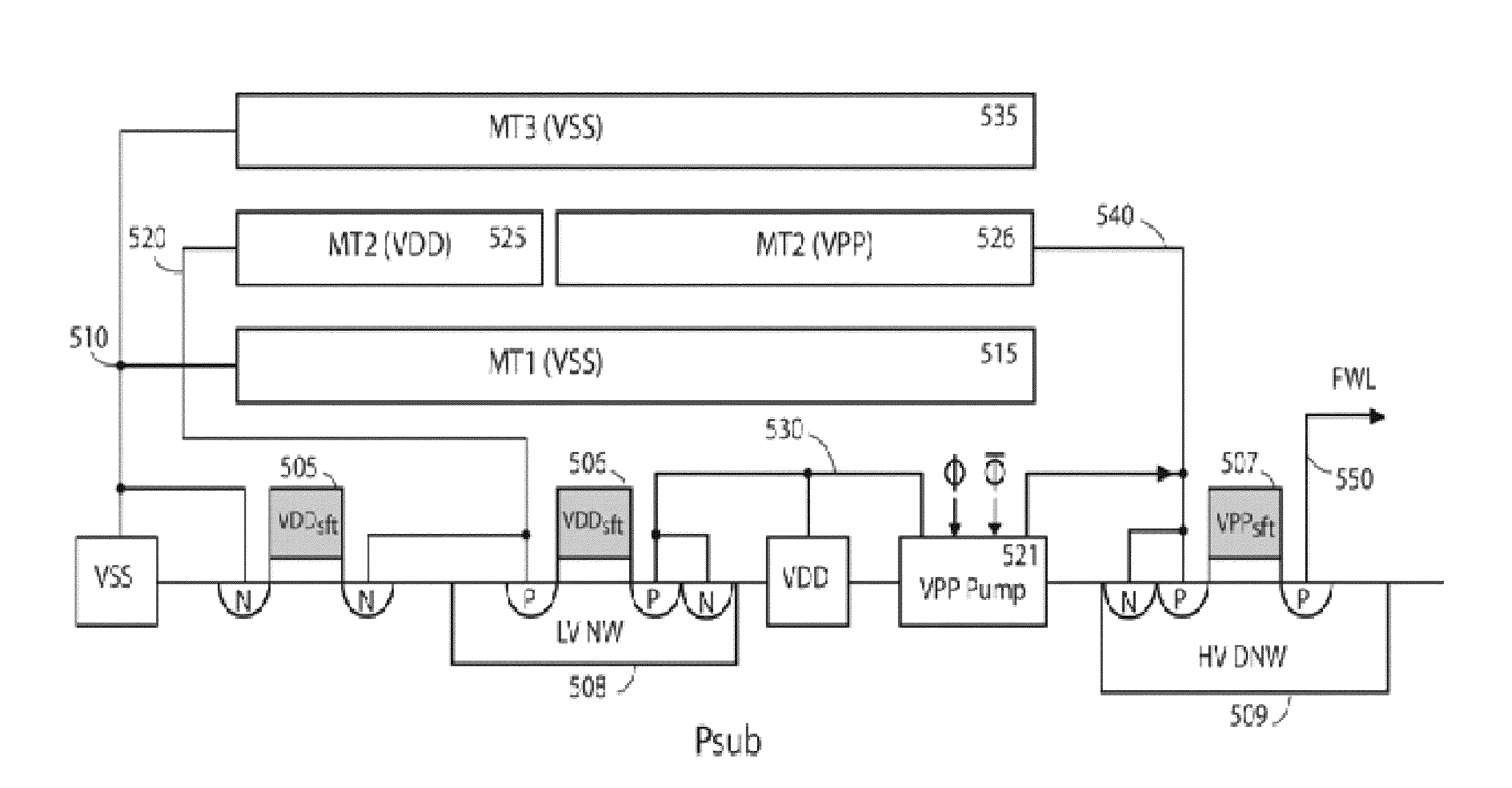
[0064]The present invention generally relates to a preferred method to improve the efficiency of the low-current VPP or VNN program operation, depending on the definition of the erase and program operation by using the on-chip HV capacitor and LV VCC capacitor for next-generation NVSRAM memory system circuit design upon VCC power loss.

[0065]It is more specifically relates to a faster three preferred on-chip always fully-charged capacitors of VPPcap, VNNcap and VCCcap as an alternative positive high voltage (+HV) or negative high voltage (−HV) and a LV power VCC supplies without using the costly and bulky Vcap and Vbat. If the defined program operation uses a +HV VPP to perform FN-channel program to selectively increase the flash cell's Vt, then the present invention prefers to form two on-chip capacitors of VPPcap and VCCcap as a back-up +HV and LV VCC supplies for an instant program operation. In contrast, if the defined program operation is reversely using −HV VNN to perform the F...


PUM


Abstract

Two on-chip capacitors including one HV capacitor VPPcap and one LV VCC capacitor VCCcap are built over a NVSRAM memory chip as a back-up second power supplies for each NVSRAM cell, regardless of 1-poly, 2-poly, PMOS or NMOS flash cell structures therein. The on-chip HV and LV capacitors are preferably made from one or more MIM or MIP layers for achieving required capacitance. A simplified VCC power system circuit without a need of a State machine designed for performing only one NVSRAM Program operation without Erase operations is proposed for initiating NVSRAM's Auto-Store operation without using any off-chip Vbat and Vcap. During the Auto-Store operation, all HV pumps and oscillators associated with the two on-chip capacitors are shut off once VCC voltage drop is detected by a VCC detector to be below 80% of regular VDD level.

Description

CROSS-REFERENCE TO RELATED APPLICATIONS[0001]This application claims priority to U.S. Patent Application No. 61 / 714,186, filed on Oct. 15, 2012, commonly assigned, and hereby incorporated by reference in its entirety herein for all purposes.[0002]This application is related to U.S. Pat. No. 7,164,608, and U.S. patent application Ser. No. 14 / 037,356, commonly assigned, which are incorporated by reference herein for all purposes.[0003]Additionally, this application is related to U.S. Pat. Nos. 5,065,362 and 7,760,540.TECHNICAL FIELD OF THE INVENTION[0004]The present embodiments relate to several improvements of conventional NVSRAM's Auto-Store” operation upon VCC power loss by adding two on-chip instant VPP and VCC power supplies, carefully designed VPP and VCC internal power buses, the low-power VPP and VCC switching circuits as well as a well-designed reduced logic control steps without any state-machine to perform single function of Auto-Store operation.[0005]The preferred on-chip ...

Claims


Application Information

Patent Timeline
Patent Type & Authority Applications(United States)
IPC IPC(8): G11C16/30G11C5/14
CPCG11C5/141G11C16/30G11C14/0063G11C16/12G11C16/22
Inventor LEE, PETER WUNGTSAO, HSING-YA
Owner APLUS FLASH TECH
Why Eureka
Try Eureka