Enhancing efficiency in solar cells by adjusting deposition power

a technology of solar cells and deposition power, applied in the direction of coatings, chemical vapor deposition coatings, semiconductor devices, etc., can solve problems such as reducing solar cell efficiency, and achieve the effect of improving device efficiency

Inactive Publication Date: 2014-05-01
INT BUSINESS MASCH CORP +1
View PDF15 Cites 3 Cited by
  • Summary
  • Abstract
  • Description
  • Claims
  • Application Information

AI Technical Summary

Benefits of technology

[0007]Methods for forming a photovoltaic device include adjusting a deposition power for depositing a buffer layer including germanium on a transparent electrode. The deposition power is configured to improve device efficiency. A p-type layer is formed on the buffer layer. An intrinsic layer and an n-type layer are formed over the p-type layer.
[0008]Another method for forming a photovoltaic device includes forming a transparent electrode on a transparent substrate, the transparent electrode having a first Fermi level; adjusting a deposition power for depositing a buffer layer including germanium on the transparent electrode, the deposition power being configured to improve device efficiency, the buffer layer having a Fermi level aligned with the first Fermi level; depositing a p-type layer on the buffer layer, the p-type layer having a conduction band level aligned with a conduction band level of the buffer layer; forming an intrinsic layer on the p-type layer; and forming an n-type layer on the intrinsic layer.
[0009]Yet another method for forming a photovoltaic device includes forming a transparent electrode on a transparent substrate, the transparent electrode having a first Fermi level; depositing a buffer layer including germanium on the transparent electrode, the buffer layer having a Fermi level substantially aligned with the first Fermi level; adjusting a deposition power for forming a p-type layer on the buffer layer, the deposition power being configured to improve device efficiency, the p-type layer having a conduction band level aligned with a conduction band level of the buffer layer; forming an intrinsic layer on the p-type layer; and forming an n-type layer on the intrinsic layer.
[0010]Still another method for forming a photovoltaic device includes forming a transparent conductive oxide on a transparent substrate; adjusting a first deposition power for depositing a buffer layer including germanium on the transparent electrode, the first deposition power being configured to improve device efficiency; adjusting a second deposition power for depositing a p-type amorphous layer on the buffer layer such that the second deposition power is configured to improve device efficiency; forming an amorphous silicon intrinsic layer on the p-type layer; forming an amorphous silicon n-type layer on the intrinsic layer; and forming a back reflector on the n-type layer.

Problems solved by technology

Both semiconductor-semiconductor band offset and semiconductor-electrode Schottky barrier decrease solar cell efficiency.

Method used


Image

  • Enhancing efficiency in solar cells by adjusting deposition power
  • Enhancing efficiency in solar cells by adjusting deposition power
  • Enhancing efficiency in solar cells by adjusting deposition power

Examples


Embodiment Construction

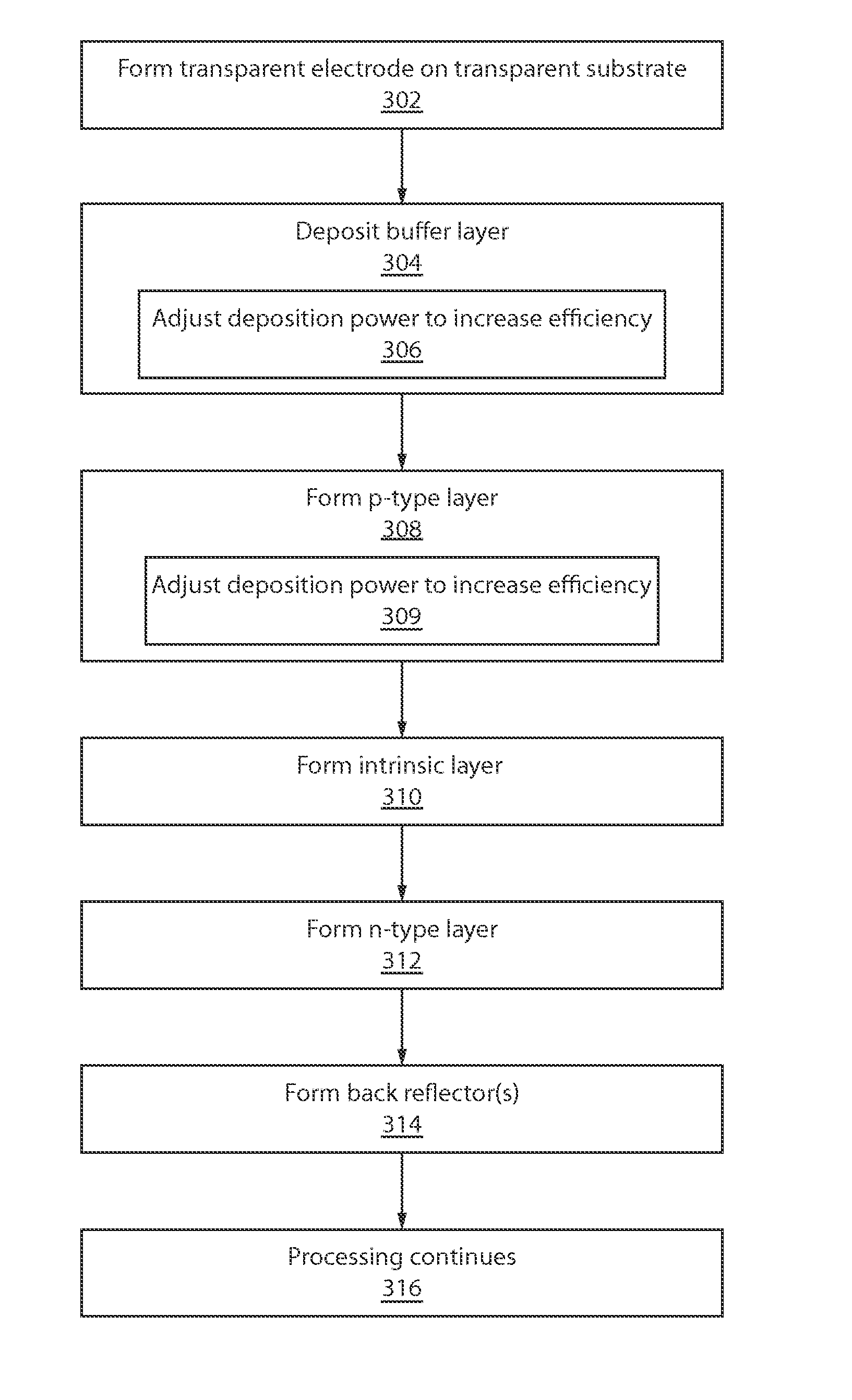
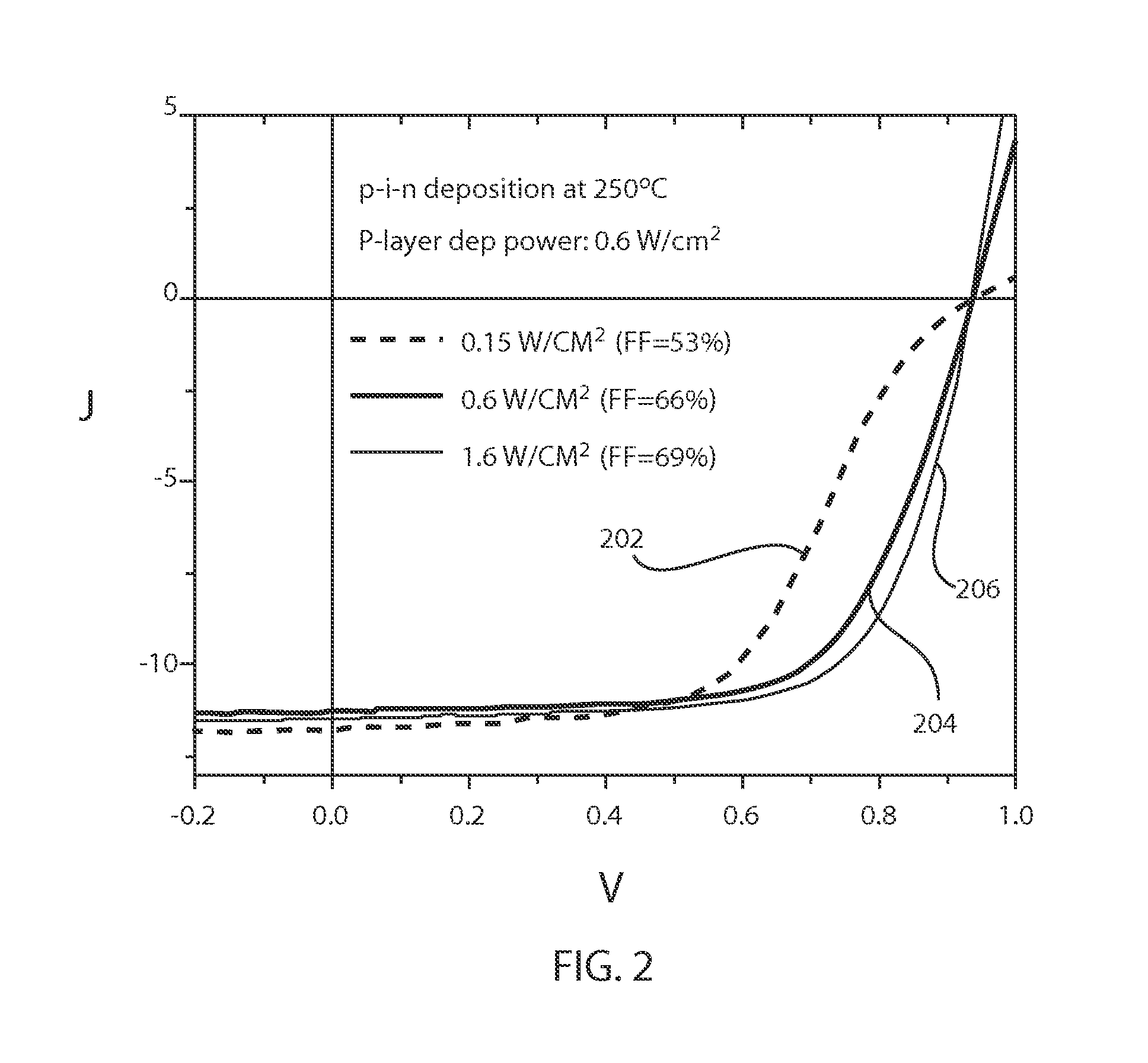
[0019]In accordance with the present principles, methods and devices are presented that provide improved efficiency based upon deposition parameters of a buffer layer formed between layers of a photovoltaic device. A band offset at a p-i interface and / or at a transparent conductive oxide (TCO) to p+ interface is adjusted to provide improved solar devices.

[0020]Band offset at the TCO / p+ layer is unavoidable since all developed TCO films are n-type. In particularly useful embodiments, photovoltaic devices are constructed using materials and processes that adjust deposition power for the formation of a buffer layer at the TCO / p+ interface. In one example, a device is provided which has a minimized band offset at a p-doped layer to intrinsic layer (p-i) interface. In another example, a buffer layer is deposited between the TCO and the p+ layer of the device using a deposition process designed to improve device efficiency. To provide improved efficiency, the manner in which the buffer la...


PUM

PropertyMeasurementUnit
temperatureaaaaaaaaaa
thicknessesaaaaaaaaaa
Fermi levelaaaaaaaaaa

Abstract

Methods for forming a photovoltaic device include adjusting a deposition power for depositing a buffer layer including germanium on a transparent electrode. The deposition power is configured to improve device efficiency. A p-type layer is formed on the buffer layer. An intrinsic layer and an n-type layer are formed over the p-type layer.

Description

RELATED APPLICATION INFORMATION[0001]This application is related to commonly assigned application Ser. No. 13 / 407,006, filed on Feb. 28, 2012 and incorporated herein by reference.[0002]This application is a Continuation application of co-pending U.S. patent application Ser. No. 13 / 406,970 filed on Feb. 28, 2012, incorporated herein by reference in its entirety.BACKGROUND[0003]1. Technical Field[0004]The present invention relates to photovoltaic devices and methods for fabrication, and more particularly to devices, structures and fabrication methods that improve efficiency by adjustment of deposition power of a buffer layer and / or a p+ layer.[0005]2. Description of the Related Art[0006]A barrier height is a difference between work functions of different materials. The barrier height is affected by the type of material with which the semiconductor is in contact. A band offset is the measure of misalignment between energy levels at the interface between two solids. The offset between a...

Claims


Application Information

Patent Timeline
Patent Type & Authority Applications(United States)
IPC IPC(8): H01L31/18H01L31/20
CPCH01L31/1884H01L31/204H01L31/02167H01L31/075Y02E10/548C23C16/22
Inventor ABOU-KANDIL, AHMEDHONG, AUGUSTIN J.KIM, JEEHWANSADANA, DEVENDRA K.
Owner INT BUSINESS MASCH CORP
Why Eureka
Try Eureka