Eureka AIR delivers breakthrough ideas for toughest innovation challenges, trusted by R&D personnel around the world.

Memory controller for memory device

Inactive Publication Date: 2014-05-01
FREESCALE SEMICON INC
View PDF3 Cites 5 Cited by
  • Summary
  • Abstract
  • Description
  • Claims
  • Application Information

AI Technical Summary

Benefits of technology

The present invention relates to a system and method for generating interface signals for a memory controller. The invention addresses the problem of manually calculating and programming timing parameters for interface signals in memory devices, which is time-consuming and error-prone. The invention provides a system that automatically calculates timing parameters and interface signals based on the timing mode of the memory device, reducing the time required for generating interface signals and overcoming the limitations of existing memory controllers. The technical effect of the invention is to improve the efficiency and accuracy of generating interface signals for memory devices.

Problems solved by technology

Hence, a change in the timing mode requires newly calculating and programming the timing parameters into the memory controller, which is a time consuming and error prone task and requires multiple programming cycles of timing registers within the memory controller.

Method used


Image

  • Memory controller for memory device
  • Memory controller for memory device
  • Memory controller for memory device

Examples


Embodiment Construction

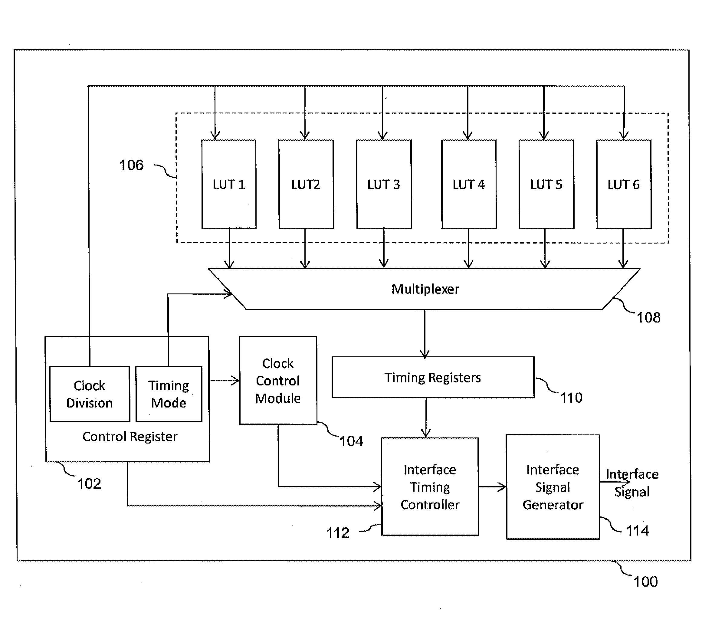
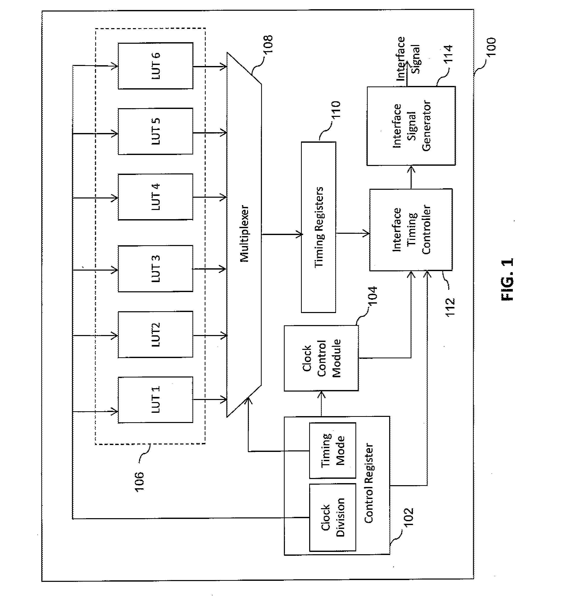
[0010]The detailed description of the appended drawings is intended as a description of the currently preferred embodiments of the present invention, and is not intended to represent the only form in which the present invention may be practiced. It is to be understood that the same or equivalent functions may be accomplished by different embodiments that are intended to be encompassed within the spirit and scope of the present invention. As used herein, the term multiplexer has been abbreviated as a mux.

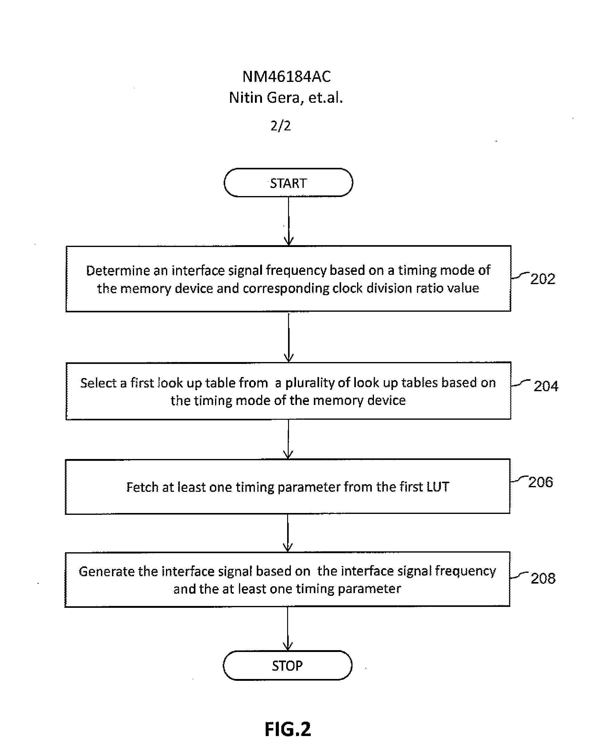
[0011]In an embodiment of the present invention, a method for generating an interface signal by a memory controller for a memory device is provided. An interface signal frequency is determined based on a timing mode of the memory device and corresponding clock division ratio value stored in the memory controller. A first look-up table (LUT) is selected from a plurality of LUTs stored in the memory controller, based on the timing mode. Each LUT stores a mapping between a clock divisio...


PUM


Abstract

A memory controller that generates interface signals for a memory device determines an interface signal frequency based on a timing mode of the memory device and a corresponding clock division ratio. Based on the timing mode, a look up table (LUT) is selected and then a timing parameter corresponding to the clock division ratio and the interface signal frequency is fetched from the LUT. An interface signal is generated based on the interface signal frequency and fetched timing parameter.

Description

BACKGROUND OF THE INVENTION[0001]The present invention relates generally to memory devices, and, more particularly, to a method and system for generating interface signals for a memory device.[0002]Electronic devices often include a memory device for storing data. Examples of memory devices include NOR and NAND flash memories, double-data rate synchronous dynamic random access memories (DDR-SDRAMs) and hard disk drives (HDDs). A memory controller is connected to the memory device and performs various operations including memory read / write operations on the memory device. Examples of memory controllers include a NOR / NAND flash controller, double data rate (DDR) 1 / 2 / 3 controllers and an integrated drive electronics (IDE) controller. The memory controllers communicate with the memory device by way of interface signals. For example, a NAND flash controller communicates with a NAND flash memory using a set of interface signals, defined by the Open NAND Flash Interface (ONFI) Working Grou...

Claims


Application Information

Patent Timeline
IPC IPC(8): G06F12/02G06F12/00
CPCG11C8/18
Inventor GERA, NITINNAUTIYAL, HEMANTRAO, AMITSINGH, PRABHJOT
Owner FREESCALE SEMICON INC
Why Eureka
Eureka Blog
Learn More