Organic light emitting display device and method of manufacturing the same

a technology of light-emitting display and organic materials, which is applied in the direction of thermoelectric device junction materials, semiconductor devices, electrical apparatus, etc., can solve the problems of low manufacturing cost, fast response time, and light-emitting display devices, and achieves the effects of improving manufacturing efficiency, reducing manufacturing costs, and improving light-emitting efficiency

Active Publication Date: 2014-05-15
LG DISPLAY CO LTD
View PDF7 Cites 37 Cited by
  • Summary
  • Abstract
  • Description
  • Claims
  • Application Information

AI Technical Summary

Benefits of technology

[0011]An aspect of the present invention is directed to a high-efficiency white organic light emitting display device (WOLED) that has a structure which emits red, green, blue, and white light by forming red, green, and blue emitting material layers as a common layer, realizes excellent light output efficiency, maintains a color characteristic, and enables the simplification of a process and the saving of the manufacturing cost.

Problems solved by technology

Furthermore, the organic light emitting display devices are driven with a low direct current (DC) voltage, have a fast response time, and are low in manufacturing cost.
During that process, the fine metal mask may not be properly aligned which may cause certain defects.
Such alignment may require substantial time and labor, which adds manufacturing expenses and lengthens manufacturing time.
Moreover, a mask used in FMM processes is costly.

Method used


Image

  • Organic light emitting display device and method of manufacturing the same
  • Organic light emitting display device and method of manufacturing the same
  • Organic light emitting display device and method of manufacturing the same

Examples


Embodiment Construction

[0019]Hereinafter, embodiments of the present invention will be described in detail with reference to the accompanying drawings. Like reference numerals refer to like elements throughout. In the following description, when the detailed description of the relevant known function or configuration is determined to unnecessarily obscure the important point of the present invention, the detailed description is not provided.

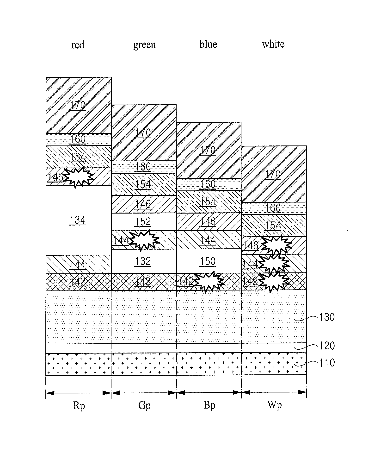
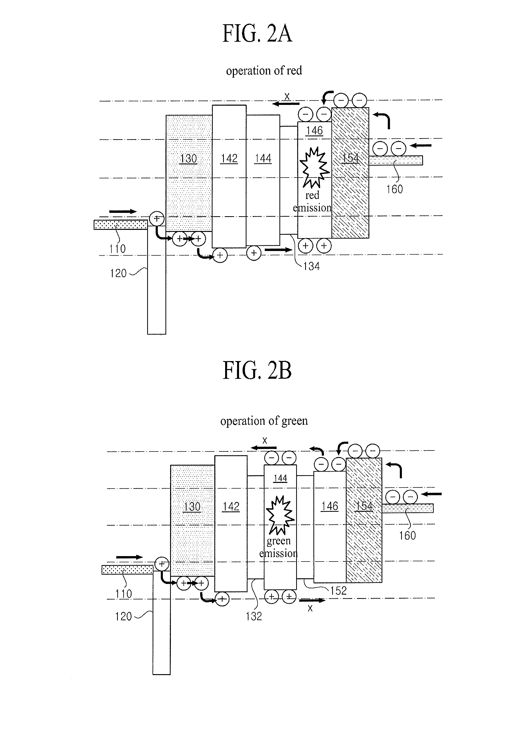
[0020]FIG. 1 is a sectional view schematically illustrating an organic light emitting display device according to one embodiment of the present invention. As illustrated in FIG. 1, the organic light emitting display device includes a first electrode (anode) 110, a hole injection layer 120, a first hole transporting layer 130, a blue common emission layer 142, a second hole transporting layer 132, a first electron transporting layer 150, a green common emission layer 144, a third hole transporting layer 134, a second electron transporting layer 152, a red common emissio...


PUM


Abstract

An organic light emitting display device includes a substrate and a plurality of pixels defined in the substrate. A pixel includes red subpixel, green subpixel, blue subpixel, and white subpixel. The organic light emitting display device includes an anode electrode formed on the substrate, a cathode electrode opposing the anode electrode, and a red common emission layer, a green common emission layer, and a blue common emission layer formed across each of the red, green, blue and white subpixel areas. The blue common emission layer is disposed above and adjacent to the anode electrode, the green common emission layer is disposed above the blue common emission layer, and the red common emission layer is disposed above the green common emission layer and adjacent to the cathode electrode.

Description

CROSS-REFERENCE TO RELATED APPLICATIONS[0001]This application claims the benefit of the Korean Patent Application Nos. 10-2012-0128572 filed on Nov. 14, 2012, and 10-2013-0057335 filed on May 21, 2013, which is hereby incorporated by reference as if fully set forth herein.BACKGROUND[0002]1. Field of the Invention[0003]The present invention relates to an organic light emitting display device and a method of manufacturing the same.[0004]2. Discussion of the Related Art[0005]As a type of new flat panel display device, organic light emitting display devices are self-emitting display devices, and have a better viewing angle and contrast ratio than liquid crystal display (LCD) devices. Also, since the organic light emitting display devices do not need a separate backlight, the organic light emitting display devices can be made lighter and thinner with excellent power consumption compared to LCD devices and the other flat panel display devices. Furthermore, the organic light emitting displ...

Claims


Application Information

Patent Timeline
Patent Type & Authority Applications(United States)
IPC IPC(8): H01L51/52H01L51/56
CPCH01L51/56H01L51/52H10K59/32H10K59/351H10K50/13H10K50/131H10K50/15H10K50/17H10K50/80H10K71/00H10K50/16H10K50/156H10K50/166H10K2102/351
Inventor PARK, JINHOKIM, KWANSOO
Owner LG DISPLAY CO LTD
Why Eureka
Try Eureka