

Through-silicon via structure with patterned surface, patterned sidewall and local isolation
a technology of through-silicon vias and silicon chips, applied in the direction of electrical equipment, semiconductor devices, semiconductor/solid-state device details, etc., can solve the problems of reducing circuit reliability, creating ever more complex package designs, and damaging circuits
- Summary
- Abstract
- Description
- Claims
- Application Information
AI Technical Summary
Benefits of technology
Problems solved by technology
Method used
Image

Examples
Embodiment Construction
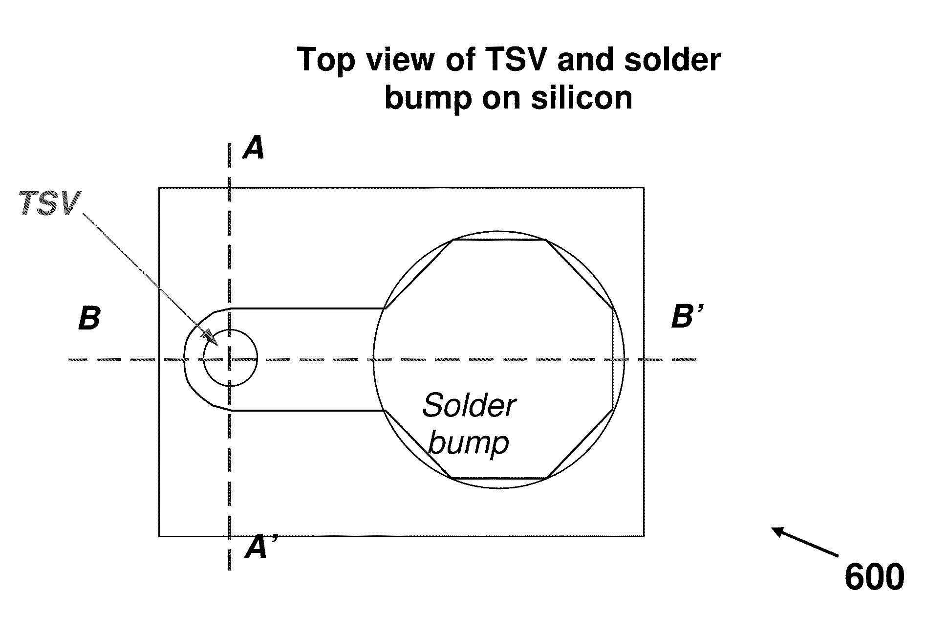
[0026]As used herein in the specification and in the appended claims, the term “via” is used in a broad sense to mean any opening in an electrical material layer or layers that allow a conductive connection between layers. Various other similar terms such as trench or channel are encompassed by the term “via” as used in describing the present invention.
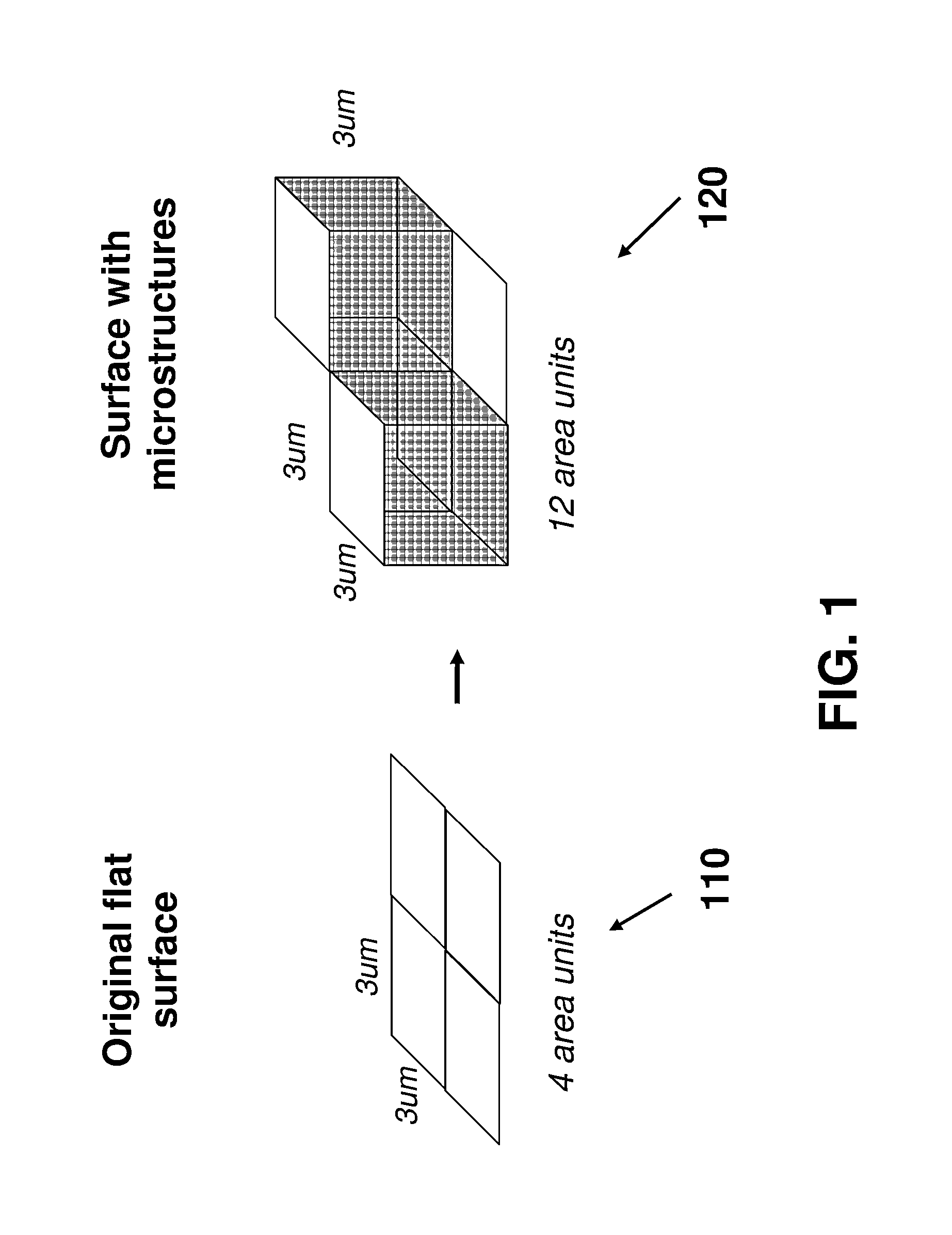
[0027]Adhesion to an isolation layer such as a polymer layer can be increased by increasing the contact area of a silicon surface on which the isolation layer is attached. According to the present invention, the contact area is increased by fabricating microstructures onto the silicon surface. FIG. 1 shows an example that the contact area can be increased by means of the microstructures. In the example shown in FIG. 1, an original flat surface 110 is composed of four squares, each measuring 3 μm×3 μm. This flat surface 110 yields a contact area of 4 area units. If two microstructures each in the form of a cube measuring 3 μm×3 μm×3 μm...
PUM
 Abstract
Description
Claims
Application Information