Multilayer chip inductor and production method for same

Inactive Publication Date: 2014-05-15
TAIYO YUDEN KK
View PDF4 Cites 14 Cited by
  • Summary
  • Abstract
  • Description
  • Claims
  • Application Information

AI Technical Summary

Benefits of technology

[0026]According to the present invention, insulator layers on which a circling pattern is formed are stacked to form a spiral coil pattern, with connection parts provided at the corners and ends of the circling pattern. Then, leader patterns are provided at the top and bottom of the coil pattern, where each leader pattern has a leader part formed at a position not overlapping with the circling parts of the coil pattern, two connection parts continuing to the leader part and corresponding to the connection parts of the circling pattern of the c

Problems solved by technology

As a result, the lamination accuracy drops due to an overall length accuracy error and alignment error between the screens that cannot be fully aligned at the time of position alignment, which is undesirable as it causes dis

Method used


Image

  • Multilayer chip inductor and production method for same
  • Multilayer chip inductor and production method for same
  • Multilayer chip inductor and production method for same

Examples


example 1

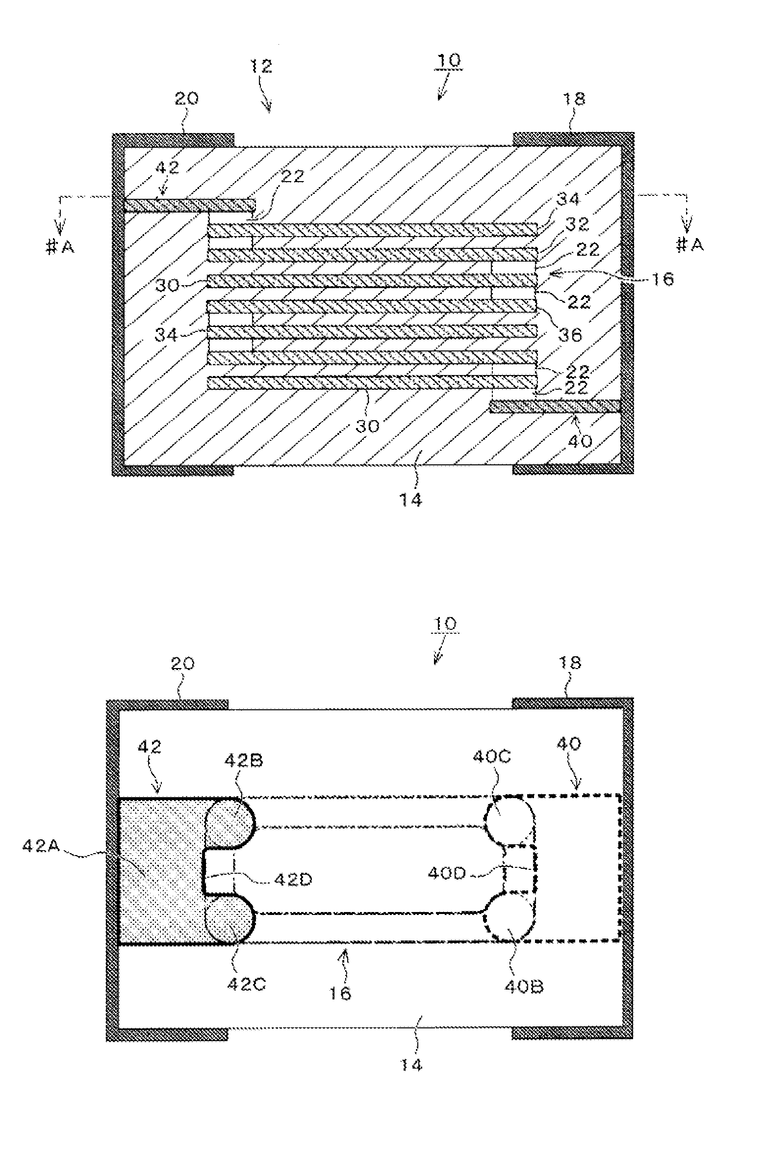
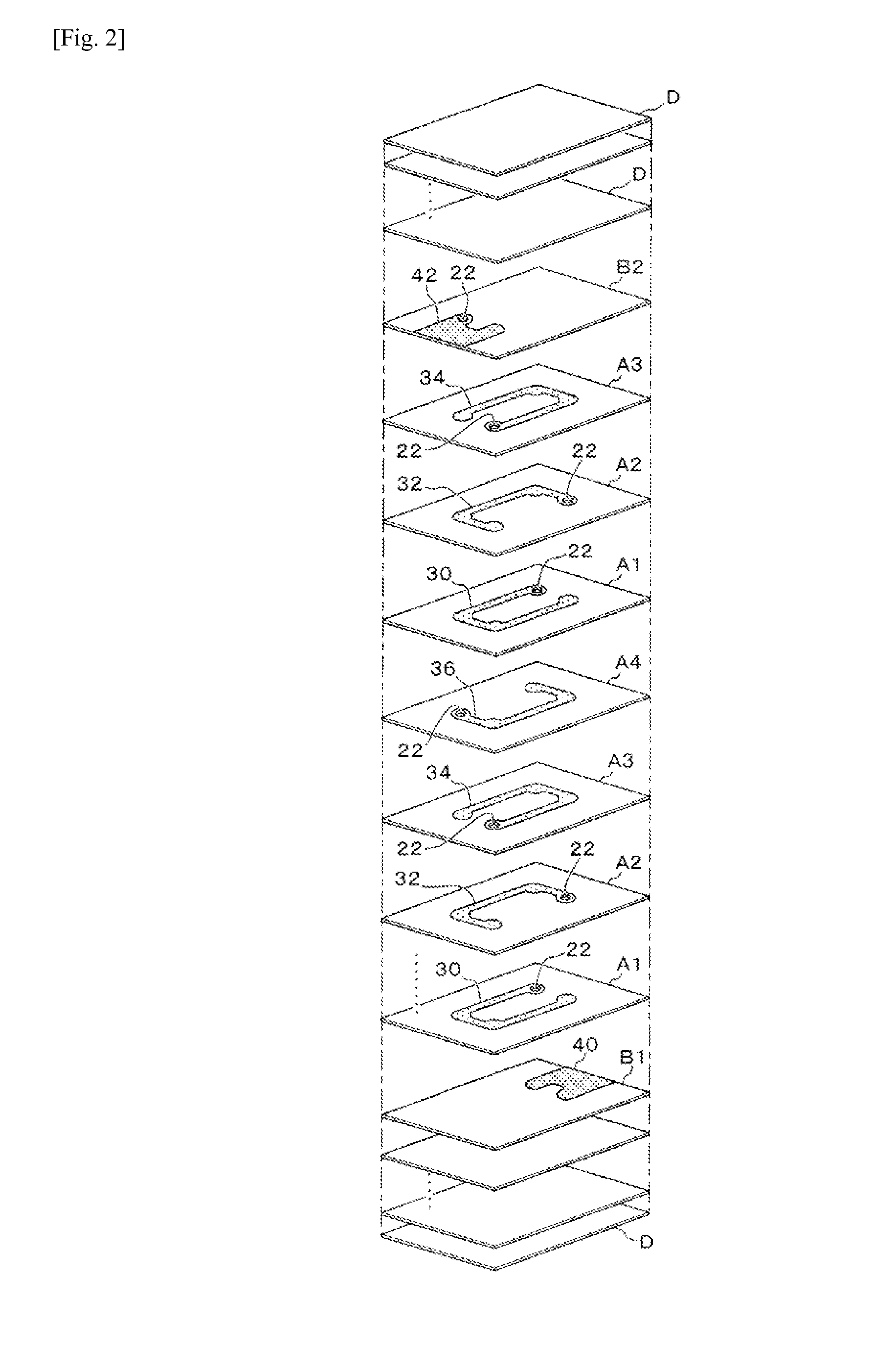
[0037]First, Example 1 of the present invention is explained by referring to FIGS. 1 to 4. FIG. 1 is a drawing showing the multilayer chip inductor in this example, where (A) is a section view of the chip that has been cut in the lamination direction, while (B) is a section view of (A) above that has been cut along line #A-#A and is viewed in the direction of the arrow. FIG. 2 is an exploded perspective view showing the sheet lamination structure according to the manufacturing process of the multilayer chip inductor in this example, while FIG. 3 is a plan view showing the circling patterns and leader patterns of the multilayer chip inductor in this example. FIG. 4 is a plan view showing how the core area of the multilayer chip inductor in this example changes, where (A) is a drawing showing a condition where displacement due to stacking does not occur, (B) is a drawing showing a condition where the circling patterns are displaced from the leader patterns, and (C) is a drawing showin...


PUM

PropertyMeasurementUnit
Magnetismaaaaaaaaaa

Abstract

A group of magnetic sheets are stacked and connected via through-holes, on each of which magnetic sheets a circling pattern having connection parts at its corners and ends is formed to form a spiral coil pattern. Leader patterns each have a leader part formed at a position not overlapping with the circling parts of the coil pattern and connected to an external terminal electrode, as well as two connection parts that continue to the leader part and are formed at positions corresponding to the connection parts of the circling patterns, together with a cutout formed between the two connection parts. Magnetic sheets with the leader patterns are provided at the top and bottom of the laminate forming the coil pattern. The multilayer chip inductor can suppress decrease in core area caused by displacement due to the stacking

Description

TECHNICAL FIELD[0001]The present invention relates to a multilayer chip inductor and method of manufacturing the same, and more specifically to suppressing any decrease in core area caused by displacement at the time of stackingBACKGROUND ART[0002]FIGS. 6 to 8 show a general structure of a conventional multilayer chip inductor. The multilayer chip inductor 100 shown in these figures comprises a magnetic body 104 in which a spiral coil pattern 106 that conductively connects multiple circling patterns 112, 114, 116, 118 via a through-hole 130 is buried. The coil pattern 106 is connected, via leader patterns 120, 124, to external terminal electrodes 108, 110 formed on the end faces of a multilayer chip 102. As shown in FIGS. 8 (E) and (F), these leader patterns 120, 124 are continuously formed with circling parts 122, 126 which are formed by conductors identical to the circling patterns 112 through 118. The circling patterns 112 through 118 and leader patterns 120, 124 have land patter...

Claims


Application Information

Patent Timeline
IPC IPC(8): H01F27/28H01F41/04
CPCH01F41/043H01F27/2804H01F17/0013H01F41/041H01F2017/0073Y10T29/4902
Inventor MARUYAMA, YOSHIKAZUKOHARA, MASATAKAOYAMA, KAZUHIKO
Owner TAIYO YUDEN KK
Why Eureka
Try Eureka