Multilayered power inductor and method for preparing the same

a power inductor and multi-layer technology, applied in the direction of transformers/inductance coils/windings/connections, inductances, coatings, etc., can solve the problems of difficult to increase capacity, difficult to implement specifications required for high current characteristics, and difficulty in implementing volume ratios of magnetic materials of 85% or more, so as to improve the capacity characteristics and increase the filling ratio of magnetic materials.

Active Publication Date: 2014-05-15
SAMSUNG ELECTRO MECHANICS CO LTD
View PDF4 Cites 19 Cited by
  • Summary
  • Abstract
  • Description
  • Claims
  • Application Information

AI Technical Summary

Benefits of technology

[0015]An object of the present invention is to provide a structure of a multilayered power inductor with im...

Problems solved by technology

However, a saturation magnetization value of the material is lower than that of a metallic material, such that it is difficult to implement specifications required for high current characteristics.
As the power inductor becomes smaller and smaller, it is difficult to increase capacity.
In this case, a volume ratio of the magnetic material may be difficult to implement 85% or more.
However, in the case of the metal powder made of the metal alloy forming the magnetic layer 10, a satura...

Method used


Image

  • Multilayered power inductor and method for preparing the same
  • Multilayered power inductor and method for preparing the same
  • Multilayered power inductor and method for preparing the same

Examples


example 1

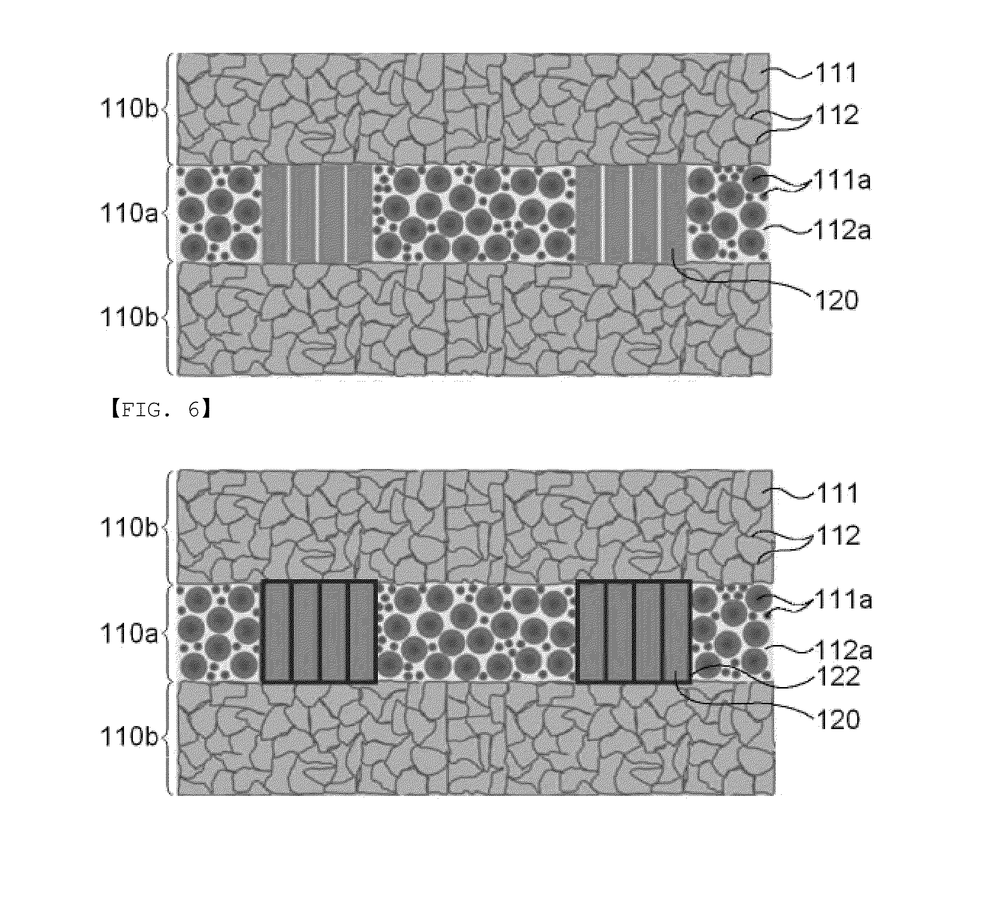
[0078]Next, according to the process of FIG. 4, the multilayered power inductor having the structure of FIG. 5 was prepared.

[0079]The magnetic body was formed by filling the same magnetic material as Comparative Example 1. Next, the magnetic bar insulation-coated with the SiO2—based ceramic material along the grain interface of the metal powder was prepared by coating the 10Si-5.5Al-84.5Fe powder having D50=25 to 40 μm and a flake shape with the SiO2—based ceramic material and thermally compressed.

[0080]The prepared magnetic bar was attached to the cover portion (upper and lower portions) of the chip body and cured, such that the magnetic layer formed of the magnetic bar is included in a part of the chip. The multilayered inductor was prepared by performing the following process in the same method as the process of Comparative Example 1.

example 2

[0081]Next, according to the process of FIG. 4, the multilayered power inductor having the structure of FIG. 5 was prepared. First, the ceramic substrate was formed with the via hole by drilling and was formed with the inner electrode coil pattern by the chemical plating. The substrate on which the inner electrode coil pattern is formed was dipped in the SiO2—based ceramic insulation coating solution to insulation coating the inner electrode coil pattern.

[0082]Further, the multilayered inductor was prepared by performing the following process in the same method as the process of Comparative Example 1, except that the magnetic layer is formed by filling the metal powder insulated with the SiO2—based ceramic material along the grain interface of the metal powder having D50=25 to 40 μm as the 10Si-5.5Al-84.5Fe having the flake shape during the magnetic filling process of the Comparative Example 1.

experimental example 1

[0083]The capacity characteristics of the multilayered power inductor prepared according to the above Comparative Example 1 and Examples 1 and 2 were evaluated and the results thereof were shown in the following Table 1. The results were obtained by preparing and measuring three samples for each specimen.

TABLE 1ComparativeExample 1Example 1Example 2Division SPL1SPL2SPL3SPL1SPL2SPL3SPL1SPL2SPL3Capacity 1.021.031.001.851.891.922.522.562.49uH)

[0084]As in the results of the above Table 1, as a result of including the metal powder insulation-coated along the grain interface of the magnetic metal powder as the magnetic layer of the multilayered power inductor according to the present invention in a part (Example 1) or the whole (Example 2) of the chip, the filling ratio of the metal powder may be increased to 90% or more within the magnetic layer and high capacity is implemented at the time of preparing the power inductor, thereby increasing the efficiency characteristics.

[0085]In additio...


PUM


Abstract

Disclosed herein are a multilayered power inductor including an inner electrode coil pattern formed on a ceramic substrate; an outer electrode layer; and a magnetic layer made of a metal powder insulated along a grain interface of the metal powder included in a part or the whole of a chip, and a method for preparing the same. According to the exemplary embodiments of the present invention, the magnetic layer made of the metal powder insulation-coated with the ceramic material along the grain interface of the magnetic metal powder can be used for a part or the whole of the chip, thereby increasing the filling ratio of the magnetic metal powder to 90% within the magnetic layer. Therefore, a high-capacity power inductor can be implemented to effectively improve efficiency characteristics.

Description

CROSS REFERENCE(S) TO RELATED APPLICATIONS[0001]This application claims the benefit under 35 U.S.C. Section 119 of Korean Patent Application Serial No. 10-2012-0128155 entitled “Multilayered Power Inductor And Method For Preparing The Same” filed on Nov. 13, 2012, which is hereby incorporated by reference in its entirety into this application.BACKGROUND OF THE INVENTION[0002]1. Technical Field[0003]The present invention relates to a multilayered power inductor and a method for preparing the same.[0004]2. Description of the Related Art[0005]As a demand for small, thin, and multi-functional electronic products is increased, a multilayered power inductor also requires large-current components. In order to improve high-current characteristics keeping pace with thinness and multi-functional characteristics, there is a need to reform a material and utilize advantages between respective materials based on complexation of the materials.[0006]In the case of the multilayered power inductor, a...

Claims


Application Information

Patent Timeline
IPC IPC(8): H01F27/255H01F27/28H01F41/12
CPCH01F27/255H01F41/127H01F27/2804H01F1/26H01F1/33H01F1/20H01F17/00H01F41/00
Inventor SHIN, SUNG SIK
Owner SAMSUNG ELECTRO MECHANICS CO LTD
Why Eureka
Try Eureka