Method for fabricating semiconductor package

a technology of semiconductor packages and thermal release tapes, applied in semiconductor devices, semiconductor/solid-state device details, electrical devices, etc., can solve the problems of reducing product reliability, high fabrication cost of thermal release tapes, and easy deviation of position of semiconductor chips, so as to avoid damage and increase product yield

Inactive Publication Date: 2014-05-15
SILICONWARE PRECISION IND CO LTD
View PDF12 Cites 6 Cited by
  • Summary
  • Abstract
  • Description
  • Claims
  • Application Information

AI Technical Summary

Benefits of technology

[0029]Therefore, by emitting light on the release layer to damage the release layer, the release layer and the carrier can be easily removed. Further, the metal layer, the adhesive layer having the metal particles dispersed therein or the adhesive layer having th

Problems solved by technology

However, a position deviation easily occurs to the semiconductor chips due to expansion of the thermal release tape when being heated and impact of the mold flow during the molding process.
As such, when a redistribution layer is formed subsequently, the redistribution layer

Method used


Image

  • Method for fabricating semiconductor package
  • Method for fabricating semiconductor package
  • Method for fabricating semiconductor package

Examples


first embodiment

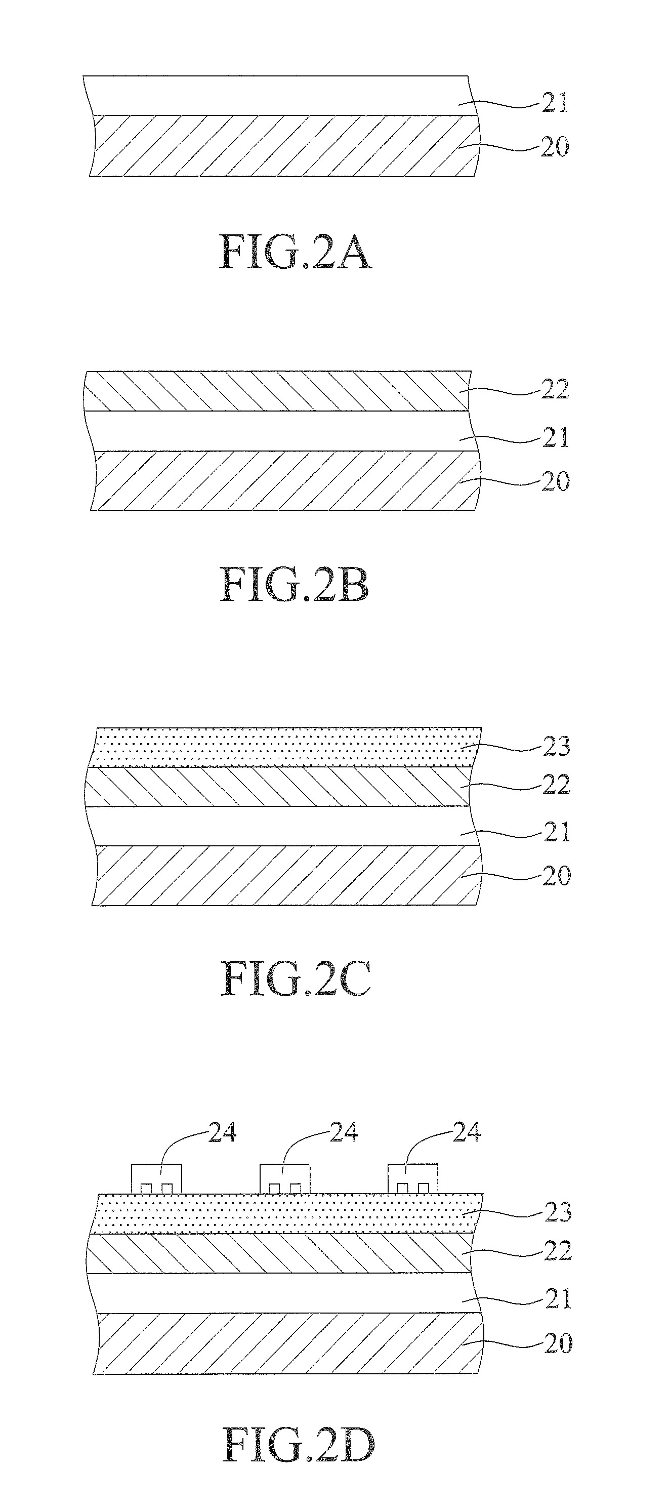
[0038]FIGS. 2A to 2H are schematic cross-sectional views illustrating a method for fabricating a semiconductor package according to a first embodiment of the present invention.

[0039]Referring to FIG. 2A, a carrier 20 is provided. The carrier 20 has a release layer 21 formed thereon. The carrier 20 can be made of glass. The release layer 21 can be made of amorphous silicon, parylene or α-SiO2. The release layer 21 can be formed through a chemical vapor deposition (CVD) process.

[0040]Referring to FIG. 2B, a metal layer 22 is formed on the release layer 21 through PECVD (Plasma Enhance Chemical Vapor Deposition), CVD, PVD (Physical Vapor Deposition) or electroless plating. In the present embodiment, the metal layer 22 is 1 μm thick. The metal layer 22 can be made of any metal.

[0041]In an alternative embodiment, the metal layer 22 can be omitted.

[0042]Referring to FIG. 2C, an adhesive layer 23 is formed on the metal layer 22.

[0043]Referring to FIG. 2D, a plurality of semiconductor chips...

second embodiment

[0048]FIG. 3 is a cross-sectional view illustrating a method for fabricating a semiconductor package according to a second embodiment of the present invention.

[0049]The present embodiment is similar to the first embodiment. A main difference of the present embodiment from the first embodiment is that the present embodiment dispenses with the metal layer 22 and instead forms an adhesive layer 23′ having a plurality of metal particles dispersed therein. The metal particles can prevent the light a from passing through the adhesive layer 23′.

third embodiment

[0050]FIG. 4 is a cross-sectional view illustrating a method for fabricating a semiconductor package according to a third embodiment of the present invention.

[0051]The present embodiment is similar to the second embodiment. The present embodiment differs from the second embodiment in that the metal particles 30 are silicon oxide balls 30a coated with metal 30b. The metal particles 30 can prevent the light a from passing through the adhesive layer 23′.


PUM


Abstract

A method for fabricating a semiconductor package is disclosed, which includes the steps of: providing a carrier having a release layer and an adhesive layer sequentially formed thereon; disposing a plurality of semiconductor chips on the adhesive layer; forming an encapsulant on the adhesive layer for encapsulating the semiconductor chips; disposing a substrate on the encapsulant; exposing the release layer to light through the carrier so as to remove the release layer and the carrier; and then removing the adhesive layer, thereby effectively preventing the semiconductor chips from being exposed to light so as to avoid any photo damage to the semiconductor chips.

Description

BACKGROUND OF THE INVENTION[0001]1. Field of the Invention[0002]The present invention relates to methods for fabricating semiconductor packages, and, more particularly, to a method for fabricating a semiconductor package that protects semiconductor chips from being damaged by light.[0003]2. Description of Related Art[0004]Currently, there are various types of semiconductor packages available in the market by various manufacturers. As semiconductor chips tend to become miniaturized nowadays, semiconductor processing technologies are required to be continuously improved so as to facilitate fabrication of lighter, thinner, shorter, and smaller electronic products.[0005]FIGS. 1A to 1E are schematic cross-sectional views illustrating a method for fabricating a semiconductor package as disclosed by U.S. Pat. No. 7,202,107.[0006]Referring to FIG. 1A, a carrier 10 is provided and an adhesive layer 11 made of a thermal release tape, for example, is formed on the carrier 10.[0007]Referring to...

Claims


Application Information

Patent Timeline
IPC IPC(8): H01L21/56
CPCH01L21/561H01L21/568H01L21/6835H01L2221/68381H01L23/3121H01L24/96H01L2924/12042H01L2924/00
Inventor CHI, CHIEH-YUANHUANG, JUNG-PANGCHEN, YAN-HENGHSU, HSI-CHANGCHANG, CHIANG-CHENGCHIU, SHIH-KUANG
Owner SILICONWARE PRECISION IND CO LTD
Why Eureka
Try Eureka