Manufacturing methods of semiconductor substrate, package and device

Active Publication Date: 2014-05-15
ADVANPAK SOLUTIONS PTE
View PDF1 Cites 0 Cited by
  • Summary
  • Abstract
  • Description
  • Claims
  • Application Information

AI Technical Summary

Benefits of technology

The invention provides methods for making semiconductor substrates, packages, and devices. These methods create a cavity in the substrate where a semiconductor element like a chip can be placed, resulting in a thinner overall product that can be made smaller.

Problems solved by technology

Nowadays, with the trend of miniaturization of electronic products expected by consumers, the size of the semiconductor device used in an electronic product is also limited so as to satisfy required specification.
However, under such circumstances, the size of the semiconductor device is difficult to reduce, constraining the miniaturization of the semiconductor device.
Therefore, the purpose of miniaturization is seldom achieved.
The problem about how to abate the above situation of miniaturization is an important issue in the development of semiconductor device.

Method used


Image

  • Manufacturing methods of semiconductor substrate, package and device
  • Manufacturing methods of semiconductor substrate, package and device
  • Manufacturing methods of semiconductor substrate, package and device

Examples


Embodiment Construction

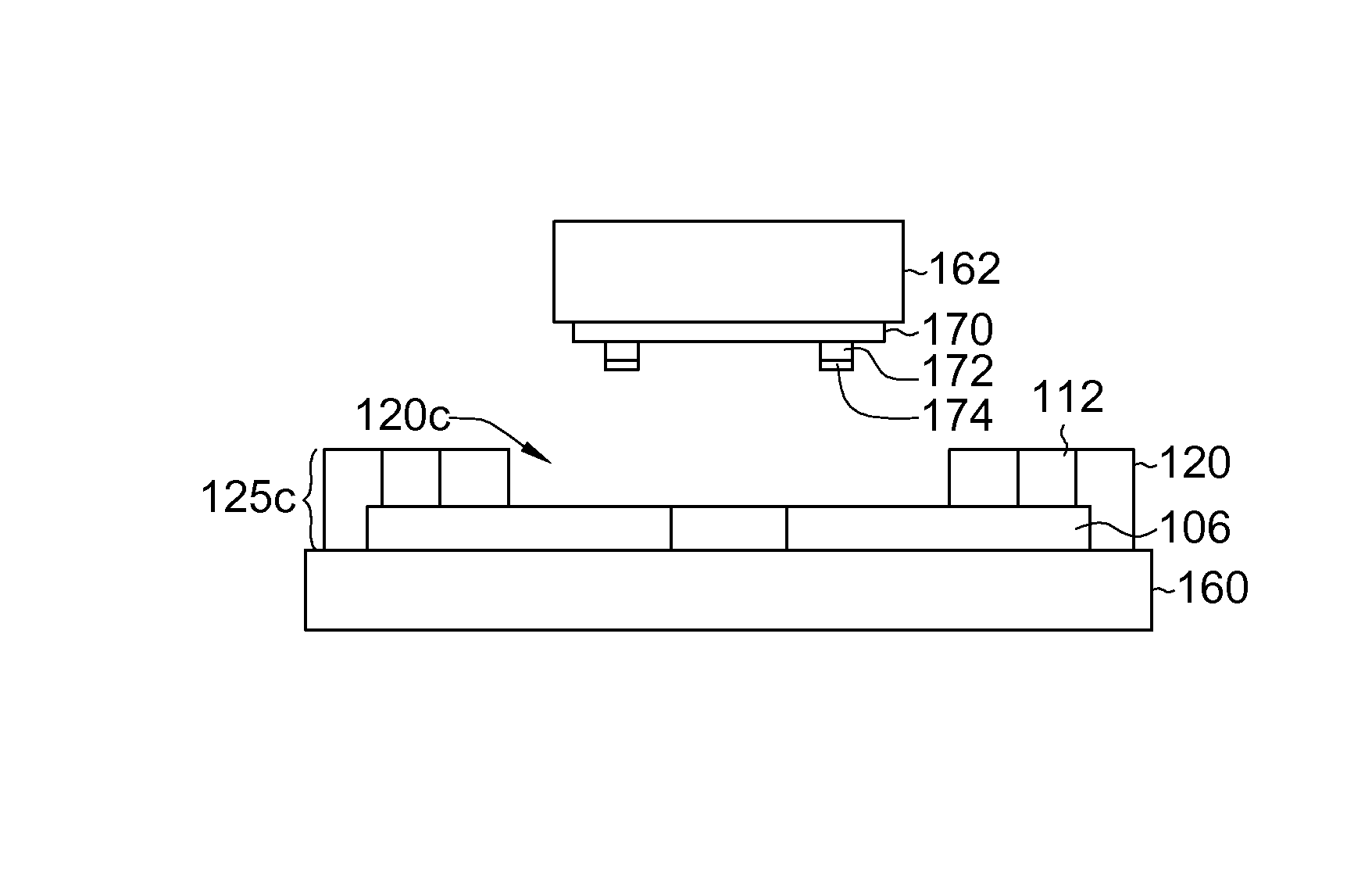
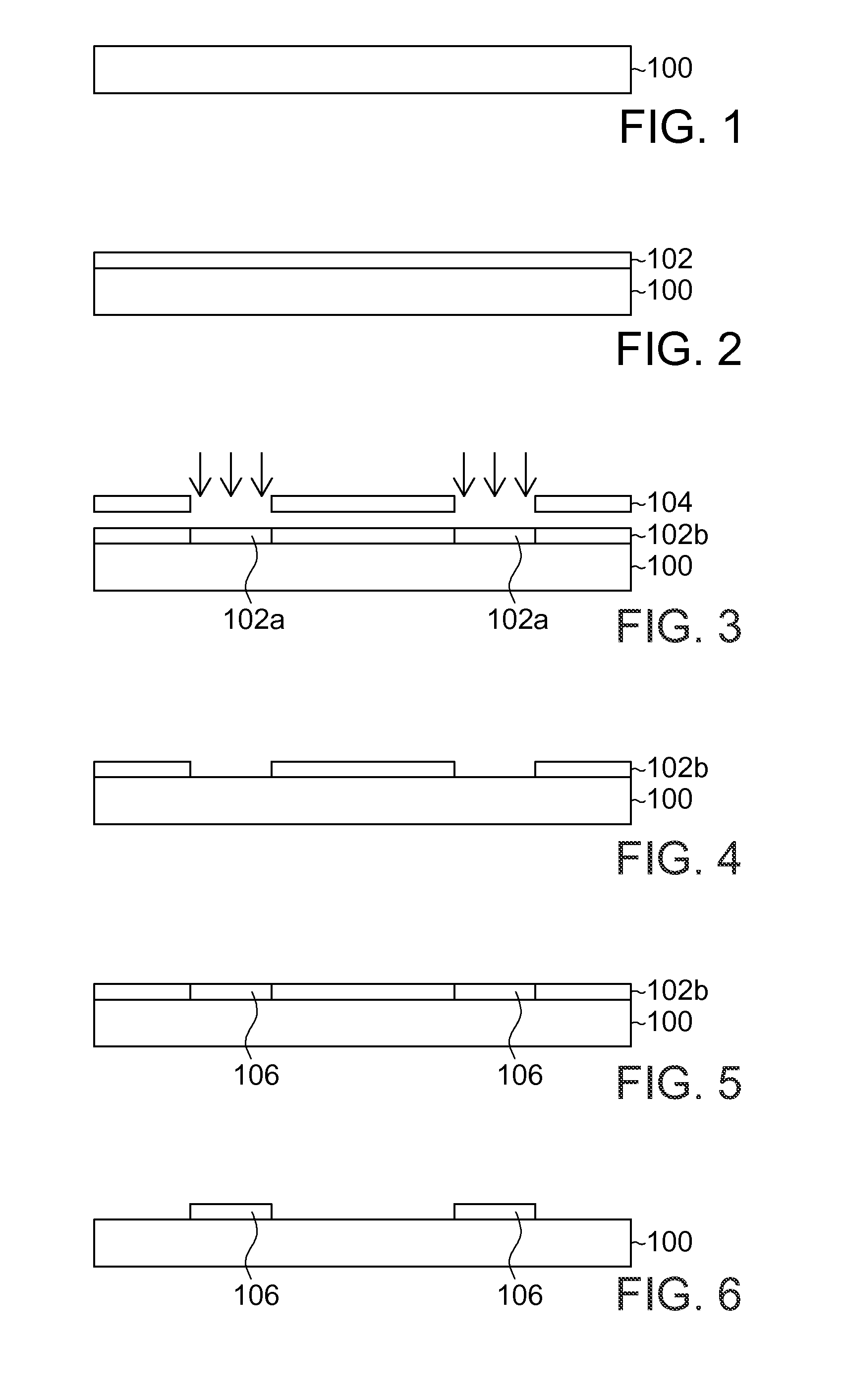
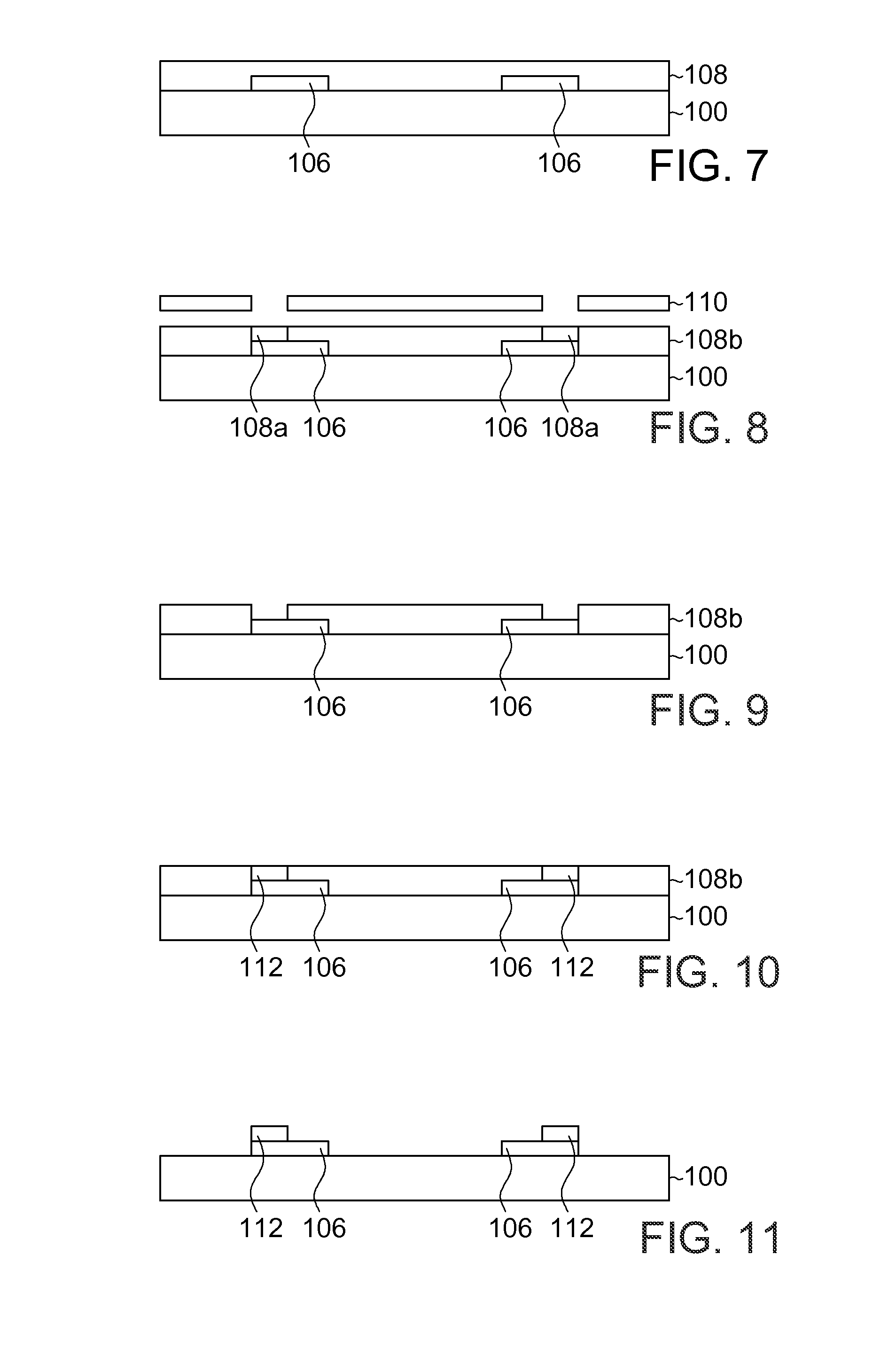
[0018]The semiconductor substrate, the semiconductor package and the semiconductor device according to the preferred embodiment of the invention, as well as their manufacturing methods, are disclosed. FIGS. 1 to 14 show the process of a manufacturing method of the semiconductor substrate.

[0019]As shown in FIG. 1, a base layer 100 is provided. The base layer 100 is preferably a conductive structure whose material is steel.

[0020]Next, as shown in FIG. 2, a photo-resist layer 102 is formed on the base layer 100. The material of the photo-resist layer 102 can be positive type resist or negative type resist.

[0021]Then, as shown in FIG. 3, the photo-resist layer 102 is patterned by, for example, lithography process. A photo mask 104 with pattern design is disposed above the photo-resist layer 102 such that the photo-resist layer 102 is selectively exposed to the radiation, and the pattern of the photo mask 104 is transferred to the photo-resist layer 102. The photo-resist layer 102 is a p...


PUM


Abstract

A manufacturing method of semiconductor substrate includes following steps: providing a base layer; forming a plurality of traces on the base layer; forming a plurality of studs correspondingly on the traces; forming a molding material layer on the base layer to encapsulate the traces and studs; forming a concave portion on the molding material layer; and, removing the base layer.

Description

[0001]This application is a divisional application of co-pending U.S. patent application Ser. No. 13 / 128,043, filed May 6, 2011 and entitled “SEMICONDUCTOR SUBSTRATE, PACKAGE AND DEVICE AND MANUFACTURING METHODS THEREOF,” which parent application claims the benefit of a provisional application Ser. No. 61 / 115,490, filed Nov. 17, 2008, and also claims the benefit of a Patent Cooperation Treaty application Serial No. PCT / SG2009 / 000428, filed Nov. 17, 2009, the subject matters of which are incorporated herein by reference.BACKGROUND OF THE INVENTION[0002]1. Field of the Invention[0003]The invention relates in general to manufacturing methods of semiconductor substrate, semiconductor package and semiconductor device.[0004]2. Description of the Related Art[0005]Nowadays, with the trend of miniaturization of electronic products expected by consumers, the size of the semiconductor device used in an electronic product is also limited so as to satisfy required specification. However, the min...

Claims


Application Information

Patent Timeline
IPC IPC(8): H01L21/48
CPCH01L21/4832H01L23/49861H01L25/105H01L2224/32225H01L2224/73204H01L23/49827H01L21/4846H01L21/563H01L23/24H01L23/3107H01L2225/1088H01L2225/1023H01L2225/1058H01L23/3135H01L2224/16227H01L2924/15153H01L2924/15321H01L2224/16225H01L23/13H01L2924/00
Inventor LIM, SHOA-SIONGLIM, KIAN-HOCK
Owner ADVANPAK SOLUTIONS PTE
Why Eureka
Try Eureka