PCB pad for imager of vehicle vision system

a vehicle vision system and imager technology, applied in the field of vehicles with cameras, can solve the problems of insufficient self-alignment during soldering, inaccurate positioning of smd chips with several legs or solder pads, etc., and achieve the effect of improving the soldering of the componen

Active Publication Date: 2014-05-22
MAGNA ELECTRONICS
View PDF3 Cites 54 Cited by
  • Summary
  • Abstract
  • Description
  • Claims
  • Application Information

AI Technical Summary

Benefits of technology

[0004]The present invention provides a vision system that utilizes one or more cameras or image sensors to capture image data of a scene exterior (such as forwardly) of a vehicle and provides a display of images indicative of or representative of the captured image data. The imager or camera includes a circuit board at wh

Problems solved by technology

A concern with such known pads is that the positioning of SMD chips with several legs or solder pads is not always accurate.
T

Method used


Image

  • PCB pad for imager of vehicle vision system
  • PCB pad for imager of vehicle vision system
  • PCB pad for imager of vehicle vision system

Examples


Embodiment Construction

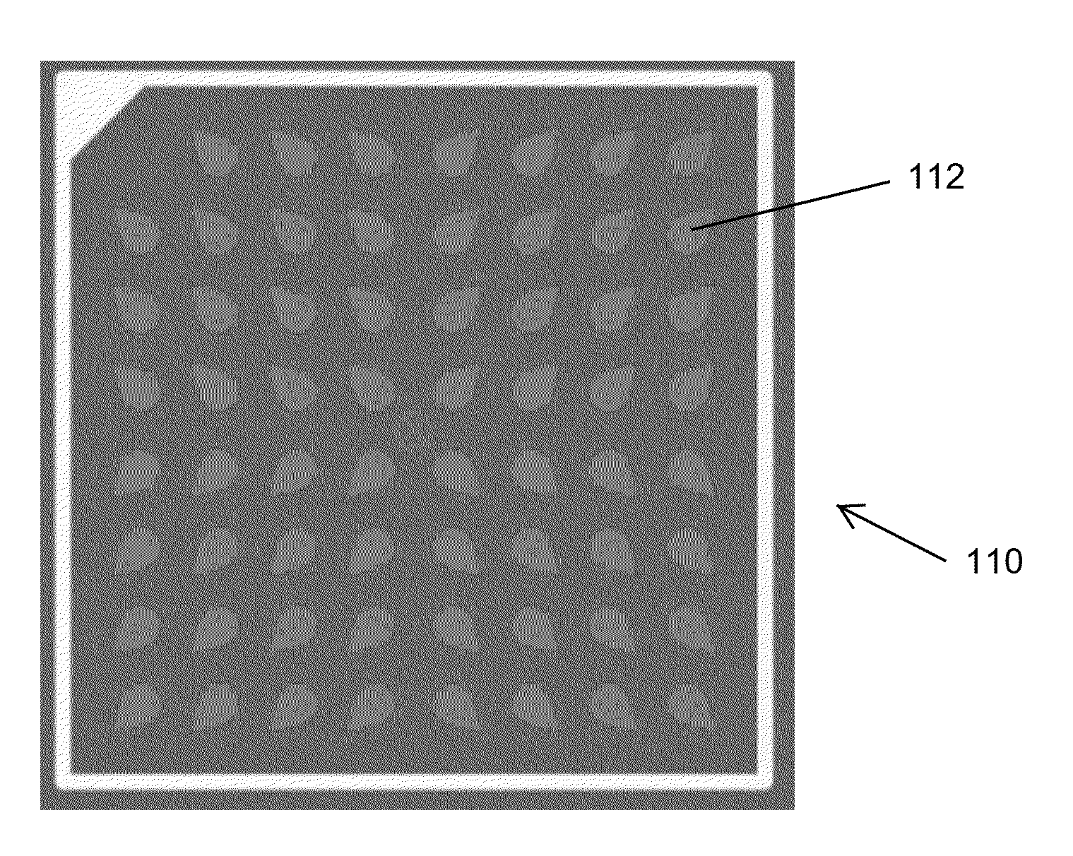
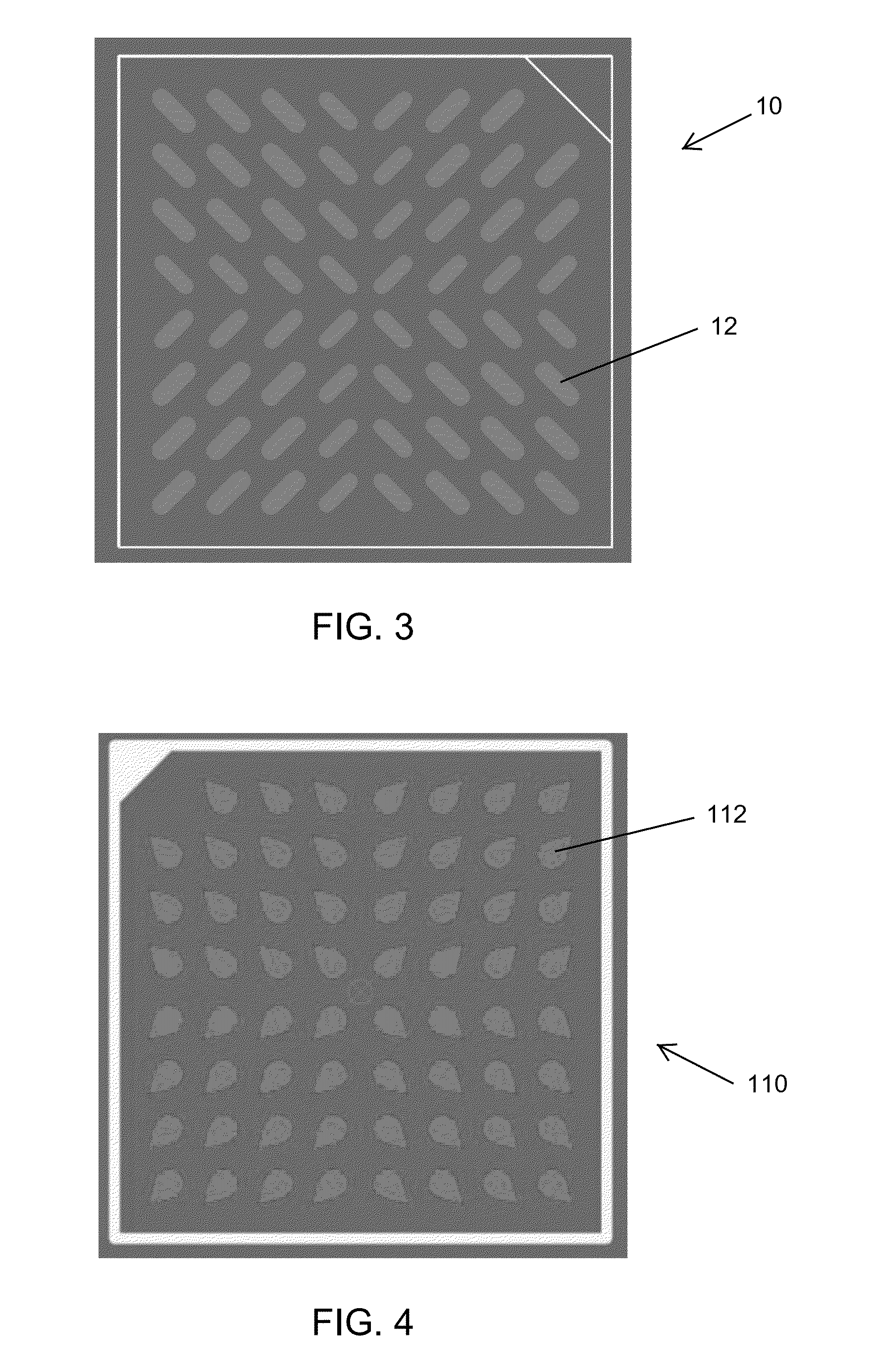
[0010]Surface mount devices (SMD) printed circuit board (PCB) solder pads of the present invention are shown in FIGS. 3 and 4 and have special designs that are meant to control the spread direction and the surface tension force direction for having a well moisting drop of solder when heating up the solder in the reflow oven. A SMD component centers between two soldering pads (in a way that the surface tension of both solder points is minimal).

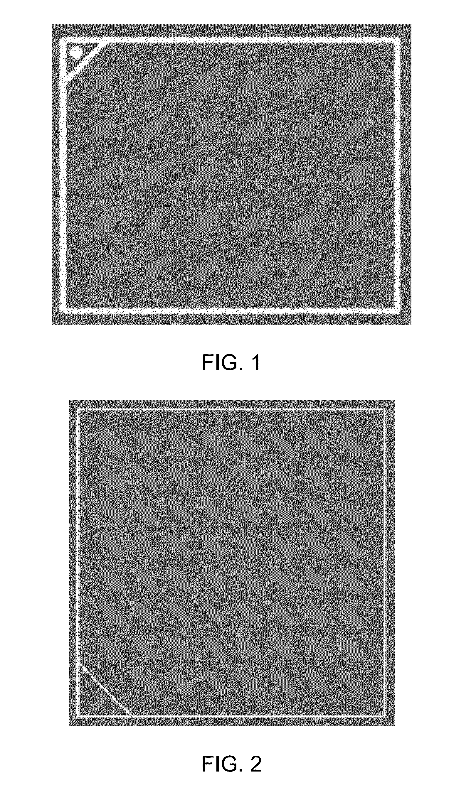
[0011]The new pad design of the present invention achieves better self adjustment results in turning and positioning alignment due to the tension forces. As shown in FIGS. 3 and 4, the pads 12, 112 of the printed circuit boards 10, 110 are configured and arranged in a non-aligned or non-parallel manner (unlike known solder pad configurations of FIGS. 1 and 2). The printed circuit board or chip of the present invention comprises an image processor chip for an image processor of a vehicle vision system that is operable to process image data captu...


PUM


Abstract

A circuit board for an image processing chip of a vision system of a vehicle is configured for a surface mount device to be attached thereto and includes at least one mounting location having a plurality of solder pads established thereat. The pads are arranged in a manner that enhances soldering of the device or component to the pad and circuit board. The pads may be arranged similarly in respective portions of the mounting location, such that the pads of one portion of the mounting location may be generally parallel to one another and may be generally orthogonal to the pads of another portion of the mounting location. Optionally, the pads may be generally tear-drop shaped, and the tear-drop shaped pads may be arranged so as to point generally towards or generally away from a center area of the mounting location of the circuit board.

Description

CROSS REFERENCE TO RELATED APPLICATION[0001]The present application claims the filing benefits of U.S. provisional application Ser. No. 61 / 727,911, filed Nov. 19, 2012, which is hereby incorporated herein by reference in its entirety.FIELD OF THE INVENTION[0002]The present invention relates to vehicles with cameras mounted thereon and in particular to vehicles with exterior-facing cameras, such as forward facing cameras and / or sideward facing cameras and / or rearward facing cameras.BACKGROUND OF THE INVENTION[0003]Use of imaging sensors in vehicle imaging systems is common and known. Examples of such known systems are described in U.S. Pat. Nos. 5,949,331; 5,670,935; and / or 5,550,677, which are hereby incorporated herein by reference in their entireties. Surface mount device (SMD) printed circuit board (PCB) pads are known and examples of known pads are shown in FIGS. 1 and 2. A concern with such known pads is that the positioning of SMD chips with several legs or solder pads is not ...

Claims


Application Information

Patent Timeline
IPC IPC(8): H05K1/11
CPCH05K2201/09381H05K2201/09418H05K1/111Y02P70/50G06V20/58B60R1/00B60R2300/8066H04N7/183H05K1/181
Inventor SIGLE, MARC
Owner MAGNA ELECTRONICS
Why Eureka
Try Eureka