Organic light emitting diode display device and method of fabricating the same

a technology of light-emitting diodes and display devices, which is applied in the manufacture of electrode systems, electric discharge tubes/lamps, discharge tubes luminescnet screens, etc., can solve the problems of increased display device sizes, shadow mask sags, and uniform deposition of large display devices

Active Publication Date: 2014-05-22
LG DISPLAY CO LTD
View PDF12 Cites 43 Cited by
  • Summary
  • Abstract
  • Description
  • Claims
  • Application Information

AI Technical Summary

Problems solved by technology

However, the shadow mask sags because the shadow mask becomes larger with an increase in sizes of display devices.
As a result, there is a problem in deposition uniformity in the larger display device.
In addition, since a shadow effect is generated in the thermal deposition method using the shadow mask, it is very difficult to fabricate a high resolution OLED display device, e.g., above 250 PPI (pixels per inch).
In addition, the OLED display device is degraded fast due to the difference in thicknesses, and the lifetime of the OLED display device is shortened.

Method used


Image

  • Organic light emitting diode display device and method of fabricating the same
  • Organic light emitting diode display device and method of fabricating the same
  • Organic light emitting diode display device and method of fabricating the same

Examples


Embodiment Construction

[0030]Reference will now be made in detail to the preferred embodiments, examples of which are illustrated in the accompanying drawings.

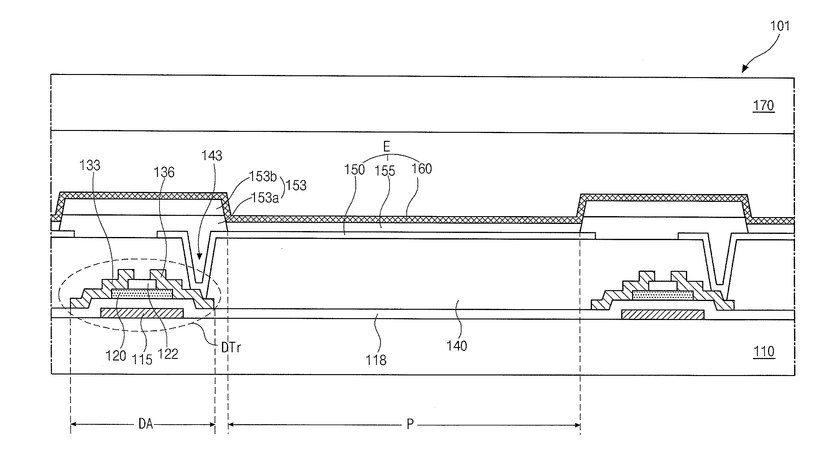
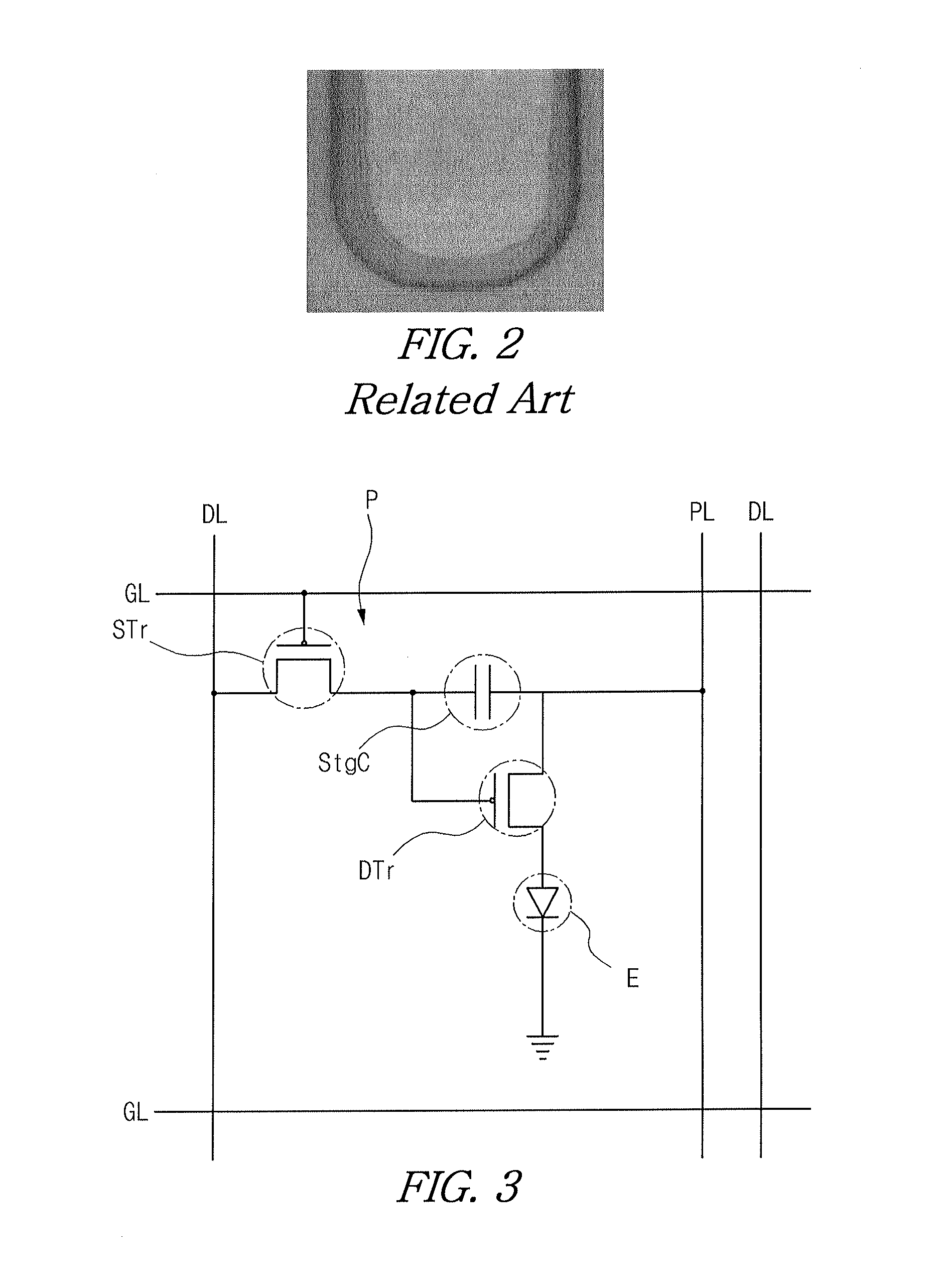
[0031]FIG. 3 is a circuit diagram of one pixel region of an OLED device.

[0032]As shown in FIG. 3, an OLED display device includes a switching thin film transistor (TFT) STr, a driving TFT DTr, a storage capacitor StgC and an emitting diode E in each pixel region P.

[0033]On a substrate (not shown), a gate line GL along a first direction and a data line DL along a second direction are formed. The gate line GL and the data line DL cross each other to define the pixel region P. A power line PL for providing a source voltage to the emitting diode E is formed to be parallel to and spaced apart from the data line DL.

[0034]The switching TFT STr is connected to the gate and data lines GL and DL, and the driving TFT DTr and the storage capacitor StgC are connected to the switching TFT STr and the power line PL. The emitting diode E is connected to the driving...


PUM


Abstract

An organic light emitting diode display device includes a first substrate including a display region, wherein a plurality of pixel regions are defined in the display region; a first electrode over the substrate and in each of the plurality of pixel regions; a bank on edges of the first electrode and surrounding each of the plurality of pixel regions, the bank including a lower layer having a hydrophilic property and an upper layer having a hydrophobic property; an organic emitting layer on the first electrode and in each of the plurality of pixel regions surrounded by the bank; and a second electrode on the organic emitting layer and covering an entire surface of the display region.

Description

[0001]The present application claims the benefit of Korean Patent Application No. 10-2012-0131546 filed in Korea on Nov. 20, 2012, which is hereby incorporated by reference for all purposes as if fully set forth herein.BACKGROUND[0002]1. Field of the Disclosure[0003]The disclosure relates to an organic light emitting diode (OLED) display device, which may be referred to as an organic electroluminescent display device, and more particularly, to an OLED display device having a bank of a double-layered structure and a method of fabricating the same.[0004]2. Discussion of the Related Art[0005]An OLED display device of new flat panel display devices has high brightness and low driving voltage. The OLED display device is a self-emitting type and has excellent view angle characteristics, contrast ratio, a response time, etc.[0006]Accordingly, the OLED display device is widely used for a television, a monitor, a mobile phone, etc.[0007]The OLED display device includes an array element and a...

Claims


Application Information

Patent Timeline
Patent Type & Authority Applications(United States)
IPC IPC(8): H05B33/20H05B33/10
CPCH10K59/122H10K71/135H10K59/1201H10K59/121H10K59/1213H10K71/00H10K59/124
Inventor JEON, HONG-MYEONGLEE, JAE-KISEO, HWANG-UNLEE, A-RYOUNGLEE, GEUM-YOUNG
Owner LG DISPLAY CO LTD
Why Eureka
Try Eureka