
Embedded non-volatile memory

a non-volatile memory and embedded memory technology, applied in the direction of semiconductor devices, diodes, electrical devices, etc., can solve the problem of the most expensive class of masks

Inactive Publication Date: 2014-06-12
WESTERN DIGITAL TECH INC
View PDF1 Cites 2 Cited by
  • Summary
  • Abstract
  • Description
  • Claims
  • Application Information

AI Technical Summary

Benefits of technology

The patent text is about how microcomputer chips are becoming more advanced and are starting to have non-volatile memory. This means that key data values can be stored in a separate area of memory that doesn't require power to function. The technical effect of this is that it allows for faster and more efficient operation of the microcomputer chip after power is restored without having to re-engage the setup process.

Problems solved by technology

However, in addition to CMOS' processing masks and processing steps, Flash memory requires several additional masks and their associated processing steps, whereby many of these additional masks are at the critical geometry of the overall process and therefore of the most costly class of mask.

Method used


Image

  • Embedded non-volatile memory
  • Embedded non-volatile memory
  • Embedded non-volatile memory

Examples


Embodiment Construction

[0011]Today's CMOS processes are finely tuned, complex processes that are very sensitive to being broken if changes are made. On of the largest manufacturers of CMOS logic, the Intel Corporation, addresses this sensitivity with its slogan, “Copy exactly.” In other words, even the slightest of changes can disrupt the entire process and require a re-tuning of that process. Various individual process steps and sequences are likewise very sensitive to being disrupted.

[0012]Some of the most delicate parts of the process include the silicon surface preparation of the areas of the substrate where the channels of MOS transistors are going to be put. These surfaces must be kept near perfect to avoid current leakage paths and recombination sites that would degrade performance.

[0013]Another sensitive stage is following the formation of salicided contacts to the MOS transistors as these contacts are easily damaged after formation by elevated temperatures (e.g., a temperature of 800° C. or highe...


PUM


Abstract

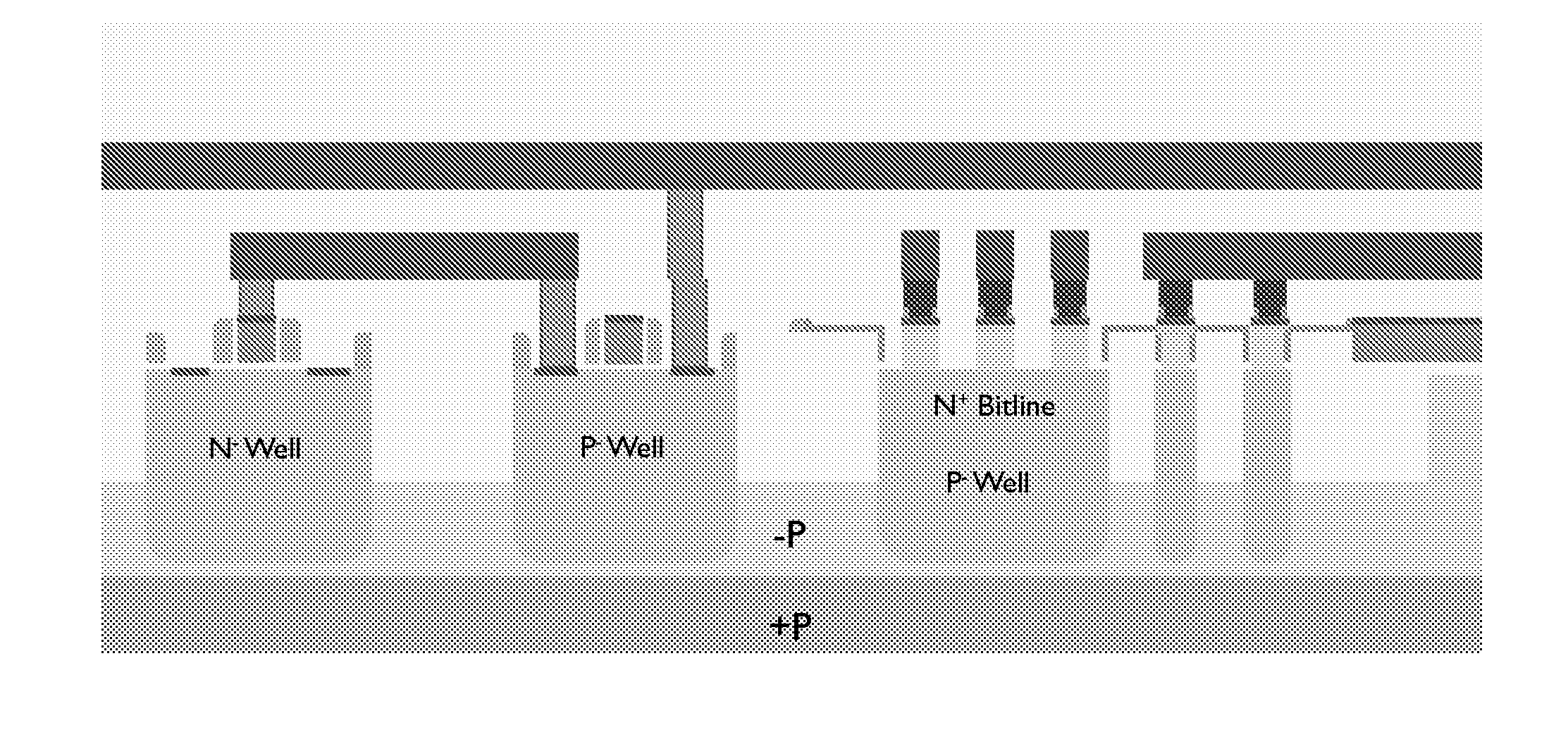
The present invention is a method of incorporating a non-volatile memory into a CMOS process that requires four or fewer masks and limited additional processing steps. The present invention is an epi-silicon or poly-silicon process sequence that is introduced into a standard CMOS process (i) after the MOS transistors' gate oxide is formed and the gate poly-silicon is deposited (thereby protecting the delicate surface areas of the MOS transistors) and (ii) before the salicided contacts to those MOS transistors are formed (thereby performing any newly introduced steps having an elevated temperature, such as any epi-silicon or poly-silicon deposition for the formation of diodes, prior to the formation of that salicide). A 4F2 memory array is achieved with a diode matrix wherein the diodes are formed in the vertical orientation.

Description

CROSS REFERENCE TO RELATED APPLICATIONS[0001]The present disclosure claims priority to Provisional Patent Application 61 / 630,297 filed on Dec. 8, 2011 by Shepard, et. al. titled “EMBEDDED NON-VOLATILE MEMORY REQUIRING ONLY FOUR MASKS” and to Provisional Patent Application 61 / 632,393 filed on Jan. 3, 2012 by Shepard, et. al. titled “EMBEDDED NON-VOLATILE MEMORY REQUIRING ONLY ONE NON-CRITICAL MASK” and those applications are hereby incorporated herein in their entirety.FIELD OF THE INVENTION[0002]The present invention relates to the manufacture and processing of semiconductors, and more particularly to the manufacture and processing of embedded memory on CMOS logic.REFERENCE TO A SEQUENCE LISTING, A TABLE, OR A COMPUTER PROGRAM LISTING COMPACT DISK APPENDIX[0003]Not Applicable.REFERENCE REGARDING FEDERAL SPONSORSHIP[0004]Not ApplicableSTATEMENT REGARDING FEDERALLY SPONSORED RESEARCH OR DEVELOPMENT[0005]Not Applicable.SUMMARY OF THE INVENTION[0006]Microcomputer chips and microcontroll...

Claims


Application Information

Patent Timeline
IPC IPC(8): H01L27/04
CPCH01L27/04H01L27/1021H10B63/20H10B63/80H10N70/231H10N70/066H10N70/8828H10N70/826H10B63/30H10N70/011H10N70/841H10N70/881H10N70/882H01L21/8238
Inventor SHEPARD, DANIEL R.APODACA, MAC D.TRENT, THOMAS MICHAELHSU, JAMES JUEN
Owner WESTERN DIGITAL TECH INC
Learn More